Introduction
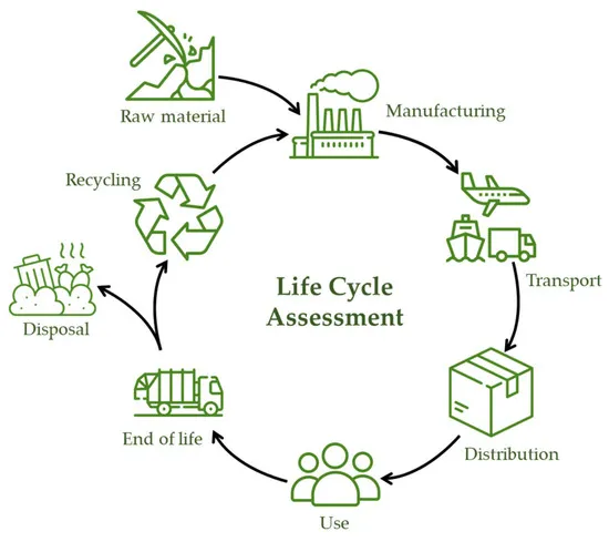
Printed circuit boards form the backbone of modern electronics, enabling everything from consumer devices to industrial systems. As demand for PCBs surges with technological advancements, their environmental impact PCBs has drawn increasing scrutiny from engineers and manufacturers alike. Key concerns include resource depletion, energy consumption during production, and challenges in end-of-life disposal. Lifecycle assessment PCB materials reveals hotspots across the supply chain, from raw material extraction to waste generation. Sustainability PCB manufacturing emerges as a critical strategy to address these issues. Recycled materials offer a practical path forward, potentially lowering emissions and conserving resources while maintaining performance standards.
Factory-driven approaches emphasize integrating eco-friendly practices without compromising reliability. Engineers must evaluate how material choices influence the overall carbon footprint. This article explores the environmental footprint of PCBs, analyzes lifecycle aspects, and details how recycled materials contribute to greener production. By focusing on factual engineering insights, it provides guidance for design and procurement teams seeking to align with sustainability goals.
Understanding the Environmental Footprint of PCBs
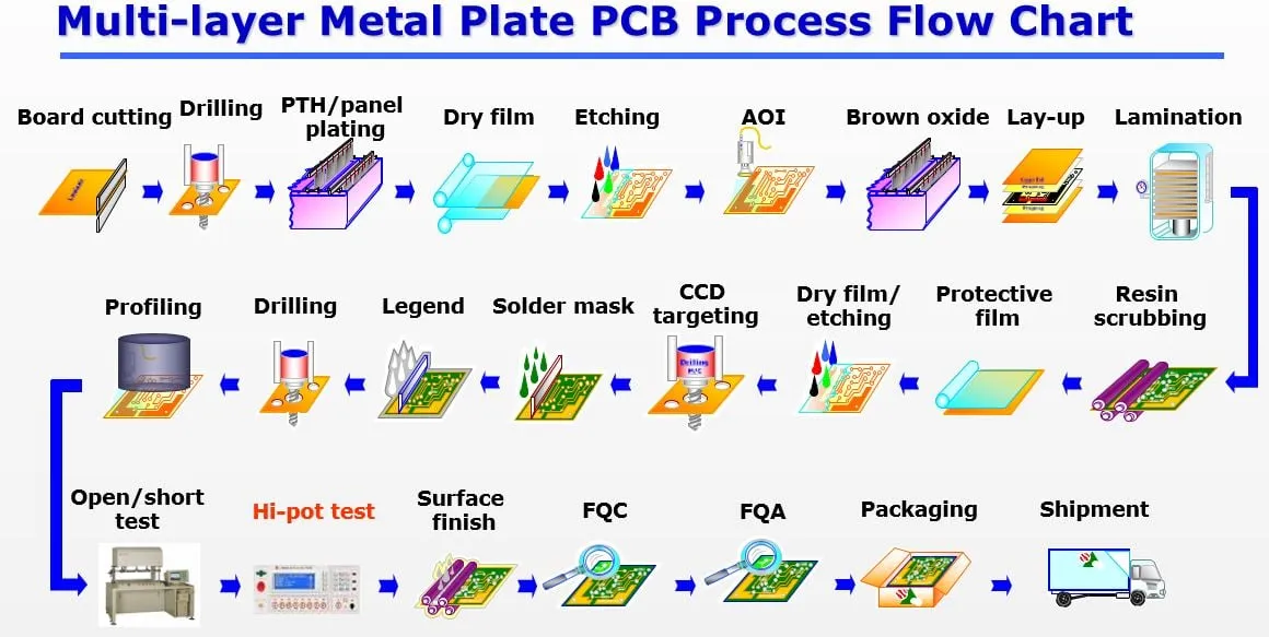
The environmental footprint of PCBs encompasses emissions, resource use, and waste across their lifecycle. Manufacturing involves energy-heavy processes like drilling, plating, and lamination, which contribute significantly to greenhouse gases. Chemical treatments for etching and surface finishing generate wastewater laden with heavy metals and acids. Improper handling leads to soil and water contamination, affecting ecosystems long-term. End-of-life PCBs, if landfilled or incinerated, release toxins such as brominated compounds into the environment.
Engineers recognize that virgin materials exacerbate these issues through mining and refining. Copper extraction alone demands vast energy and water resources. Factory operations must balance high-volume output with emission controls to mitigate local pollution. Reducing carbon footprint PCBs requires holistic strategies beyond compliance. Sustainability PCB manufacturing integrates these factors into process design for measurable improvements.
Lifecycle Assessment of PCB Materials
Lifecycle assessment PCB materials evaluates impacts from cradle to grave, covering raw material sourcing, fabrication, assembly, use, and disposal. Raw materials like copper foil, epoxy resins, and glass fibers dominate early-stage footprints due to extraction and processing. Manufacturing phases amplify energy use through heating, pressing, and electrochemical steps. During the operational phase, PCBs contribute minimally unless in high-power applications. Disposal poses risks if recycling rates remain low, as composite structures resist breakdown.
Standardized methods guide engineers in quantifying these stages. Assessments identify hotspots, such as copper production accounting for a large share of emissions. Data from factory audits inform material substitutions. Recycled inputs shift burdens downstream toward recovery rather than depletion. This approach supports informed decisions in PCB specification.
Major Contributors to the Environmental Impact of PCBs
Raw material extraction stands as a primary driver of environmental impact PCBs. Copper mining disrupts landscapes, consumes water, and emits particulates. Resin production relies on petrochemicals, tying it to fossil fuel dependency. Glass fiber weaving adds to dust and energy demands. These upstream activities set the tone for the entire chain.
Fabrication processes intensify the footprint through high electricity use in dry film lamination and electroplating. Etching solutions, often copper chloride-based, require neutralization to prevent discharge hazards. Drilling generates fine dust needing capture systems. Waste streams include panel trimmings and reject boards, complicating zero-waste goals. Engineers address these via process optimization and effluent treatment.
End-of-life management amplifies risks without proper protocols. Landfills leach metals into groundwater, while incineration volatilizes halogens. Low recycling efficiency perpetuates virgin material loops. Factory insights highlight the need for design-for-recycling features early in development.
The Role of Recycled Materials in Reducing PCB Footprints
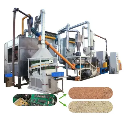
Recycled materials directly tackle environmental impact PCBs by closing material loops. Recycled copper foil, derived from scrap electronics or industrial waste, bypasses mining phases. This substitution cuts energy demands in smelting and refining, aiding reducing carbon footprint PCBs. Resins from post-consumer plastics or bio-based sources reduce reliance on non-renewables. Glass fibers reclaimed from demolished structures maintain reinforcement properties.
Environmental benefits recycled materials include lower emissions and conserved resources. Factory trials confirm compatibility with standard lamination cycles. Copper purity remains high enough for conductive traces, avoiding signal integrity issues. Composite blends enhance recyclability without delamination risks. Engineers verify performance through thermal and mechanical tests.
Best Practices for Sustainability PCB Manufacturing with Recycled Materials
Incorporate recycled content during material selection, prioritizing suppliers with traceability. Conduct incoming inspections for impurity levels that could affect plating adhesion. ISO 14001 provides a framework for environmental management systems, ensuring systematic pollution prevention. Adjust press cycles to accommodate recycled resin viscosities, preventing voids.
Quality control aligns with IPC-6012E specifications for rigid boards, validating electrical and mechanical integrity. Non-adjacent testing verifies warpage and CTE matching. Process engineers optimize etchants for recycled copper's surface characteristics. Waste minimization loops scraps back into low-spec runs.
Design for disassembly facilitates future recovery. Modular layouts ease component separation. Halogen-free formulations pair well with recycled inputs, reducing fire risks. Factory data shows these practices yield consistent yields.
Challenges in Adopting Recycled Materials and Engineering Solutions
Variability in recycled feedstock poses consistency challenges for high-reliability PCBs. Impurities may increase via defects or oxidation. Engineers mitigate via alloying or purification steps pre-foil rolling. Cost fluctuations demand long-term contracts for stability.
Performance validation requires extended reliability testing under IPC-A-600K acceptability criteria. Thermal cycling exposes CTE mismatches in hybrid laminates. Solutions include hybrid stacks blending virgin and recycled layers strategically. Supply chain transparency builds confidence in sourcing.
Future directions involve advanced recycling like hydrometallurgy for pure metal recovery. Bio-leaching emerges for low-impact extraction. Engineers collaborate on scalable pilots to refine these.
Conclusion
The environmental footprint of PCBs demands proactive strategies amid rising production volumes. Lifecycle assessment PCB materials underscores raw inputs and manufacturing as key levers for change. Recycled materials deliver environmental benefits recycled materials by slashing extraction needs and emissions. Factory-aligned practices, guided by standards like ISO 14001 and IPC-6012E, ensure viability.
Engineers play a pivotal role in specifying sustainable options without trade-offs. Reducing carbon footprint PCBs becomes feasible through informed choices. Sustainability PCB manufacturing evolves from compliance to competitive advantage. Prioritizing recycled content paves the way for resilient electronics ecosystems.
FAQs
Q1: What are the main stages in lifecycle assessment PCB materials?
A1: Lifecycle assessment PCB materials covers raw material extraction, manufacturing, use, and end-of-life disposal. Each stage quantifies energy, emissions, and waste. Factory engineers use this to pinpoint hotspots like copper refining. Recycled alternatives optimize early phases, aligning with sustainability PCB manufacturing goals.
Q2: How do recycled materials help in reducing carbon footprint PCBs?
A2: Recycled materials, especially copper, lower energy use compared to virgin mining. They reduce emissions in smelting and transport phases. Factory processes adapt seamlessly, maintaining IPC standards. Overall, they support environmental impact PCBs mitigation through closed loops. Procurement teams benefit from resource efficiency.
Q3: What environmental benefits recycled materials offer in PCB production?
A3: Environmental benefits recycled materials include conserved mining resources and decreased wastewater from processing. They minimize landfill contributions by enabling reuse. Engineers note improved traceability under ISO 14001. These inputs enhance sustainability PCB manufacturing without reliability losses. Long-term, they cut global emissions.
Q4: How can engineers ensure quality with recycled materials in PCBs?
A4: Engineers verify recycled materials via IPC-6012E qualification tests for performance. Mechanical and electrical checks confirm compatibility. Factory protocols include CTE analysis to prevent failures. Standards guide acceptance, ensuring environmental impact PCBs reductions do not compromise designs.
References
ISO 14001:2015 — Environmental management systems — Requirements with guidance for use. ISO, 2015
IPC-6012E — Qualification and Performance Specification for Rigid Printed Boards. IPC, 2017
IPC-A-600K — Acceptability of Printed Boards. IPC, 2020


