Introduction
Printed circuit boards underpin countless electronic devices, yet their production costs can quickly spiral due to overlooked design flaws. Engineers often focus on functionality during initial layouts, but manufacturing realities introduce variables like material waste, yield losses, and extended lead times. A PCB DFM review bridges this gap by scrutinizing designs against fabrication and assembly constraints early in the process. This proactive step enables PCB cost optimization DFM, turning potential expenses into savings through refined manufacturability. As electrical engineers navigate tighter budgets and faster timelines, understanding DFM's role becomes essential for sustainable project outcomes. This deep dive explores how DFM reviews deliver design for manufacturing cost savings across the PCB lifecycle.
What Is a PCB DFM Review and Why It Matters
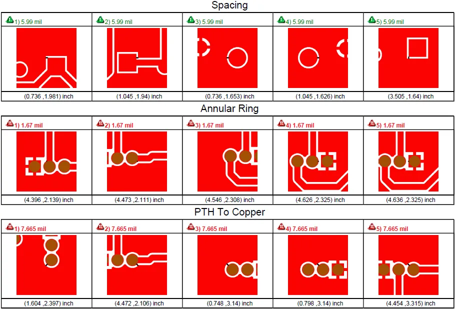
A PCB DFM review systematically evaluates a board design to ensure it aligns with practical manufacturing capabilities. It involves analyzing Gerber files, stackups, drill data, and assembly drawings against established fabrication rules. Unlike basic design rule checks in CAD software, DFM extends to factory-specific tolerances, material interactions, and process efficiencies. For instance, it flags issues like undersized vias or irregular panel outlines that could increase setup times or scrap rates.
The relevance of DFM in the PCB industry stems from its direct impact on overall costs. Poor manufacturability leads to higher defect rates, rework, and delayed shipments, amplifying expenses beyond raw materials. In high-volume production, even minor optimizations yield substantial returns; a 5 percent yield improvement can slash costs significantly. DFM cost reduction PCB strategies matter because they minimize these risks upfront, allowing procurement teams to secure competitive quotes. Engineers benefit from fewer iterations, preserving time and resources for innovation. Ultimately, integrating DFM fosters reliability while supporting PCB fabrication cost analysis for informed decision-making.
Key Technical Principles Behind DFM Cost Impacts
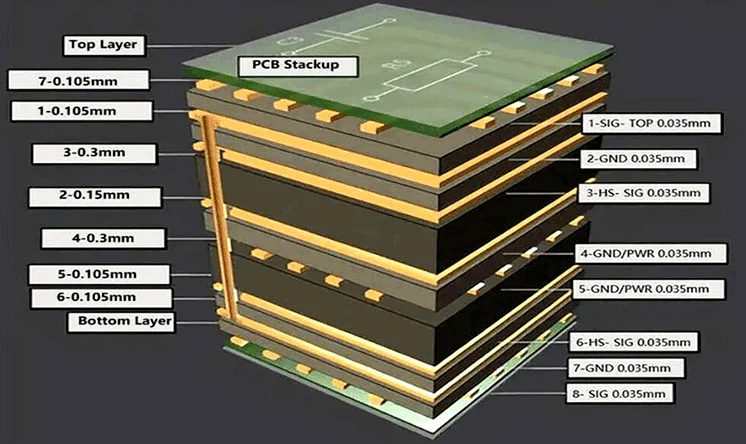
PCB costs arise from multiple fabrication stages, each influenced by design choices. Layer count directly affects material usage and pressing cycles; excess layers beyond functional needs inflate expenses without performance gains. Trace routing density impacts etching precision, where overly tight patterns demand finer resolutions and longer exposure times. Vias represent another cost driver, as blind or buried types require sequential lamination, escalating process complexity over simple through-hole designs.
Material selection plays a pivotal role in DFM analysis. Thicker copper weights enhance current handling but complicate etching and plating uniformity, potentially requiring additional chemical treatments. Board outline shapes influence panel utilization; irregular contours waste substrate area during depanelization, reducing yield per panel. Solder mask and silkscreen alignments must accommodate registration tolerances to avoid misprints that necessitate scrap. These principles highlight how design elements cascade into manufacturing economics.
Adhering to standards like IPC-6012E ensures designs meet qualification criteria for rigid boards, preventing non-conformances that drive up costs. For example, minimum annular ring requirements prevent drill breakout, safeguarding yield. Electrical test point placement affects fixture costs; insufficient or poorly spaced probes extend programming and fixturing time. Thermal management features, such as via tents, must balance coverage with solderability to avoid defects during reflow.
Drill and routing optimization forms a core DFM mechanism. Standard drill sizes, typically in 0.1 mm increments, minimize tool changes and wear, reducing setup costs. Non-standard holes trigger custom tooling, which adds fees and delays. Aspect ratios for vias, limited by plating chemistry, prevent voids if exceeded; deeper holes demand slower drill feeds, increasing cycle times. Panelization strategies maximize board count per panel while maintaining spacing for v-scoring or tab routing, directly boosting throughput.
Surface finishes influence long-term costs through shelf life and assembly compatibility. Hot air solder leveling suits cost-sensitive runs but offers less planarity than ENIG for fine-pitch components. DFM reviews quantify these trade-offs via fabrication cost analysis, projecting savings from standardized features.
Best Practices for DFM Cost Reduction in PCB Design
Engineers can implement DFM cost reduction PCB practices by prioritizing symmetry in layer stackups. Balanced copper distribution across layers minimizes warpage during lamination and reflow, adhering to flatness specs in IPC-A-600K. This reduces fixturing needs for assembly and testing, cutting ancillary expenses. Simulate stackups early to predict CTE mismatches between cores and prepregs, avoiding delamination risks that inflate rework budgets.
Optimize trace and spacing geometries for standard panel processes. Maintain clearances above minimums where possible to ease etching undercutting, enhancing yield. Group similar net lengths to streamline impedance control testing, limiting coupon requirements. For high-density interconnects, favor microvias in fanout patterns over dogbones, as they consolidate drill operations.
Incorporate assembly-friendly features during DFM review. Fiducials sized at 1 mm with clear zones aid pick-and-place accuracy, reducing offsets. Component keep-outs prevent solder bridging, while defined paste apertures ensure consistent deposits. For wave soldering, orient boards to leverage conveyor flow, minimizing manual handling. These adjustments support design for manufacturing cost savings without compromising electrical integrity.
Material and finish selections should align with volume and environment. FR-4 with standard Tg values suffices for most applications, avoiding premium high-Tg laminates unless justified by thermal cycling demands. Controlled impedance traces require precise dielectric thickness; specify tolerances that match fab capabilities to skip extra measurements.
Conduct iterative DFM checks using checklists covering fab, assembly, and test. Review bill of materials for lead-free compliance per J-STD-020E, ensuring moisture sensitivity levels match reflow profiles. Quantify impacts through yield modeling; for example, halving via count via fanout optimization can trim drill time by 20 percent. Collaborate with fabrication partners pre-tapeout to validate assumptions, refining designs for peak efficiency.
Real-World Insights from DFM Implementation
Factory-driven DFM reveals patterns in cost overruns, such as over-specifying tolerances. Tight dimensional controls beyond standard ±0.15 mm for hole positions rarely add value but trigger inspection escalations. Instead, leverage statistical process control inherent in modern fabs for relaxed specs where function permits. This shift alone can reduce metrology costs substantially.
Troubleshooting common pitfalls involves root cause analysis. Bow and twist exceeding 0.75 percent often traces to asymmetric builds; symmetrize to comply without added layers. Solder mask registration failures stem from artwork offsets; verify scales during review. These insights, drawn from production data, underscore DFM's role in preempting issues.
Conclusion
PCB DFM reviews unlock substantial cost savings by aligning designs with manufacturing realities. From stackup symmetry to standardized drills, targeted optimizations drive PCB cost optimization DFM across layers, materials, and processes. Electrical engineers gain from fewer defects, faster ramps, and competitive pricing through rigorous DFM cost reduction PCB practices. Prioritizing these steps not only trims expenses but elevates board reliability. Embrace DFM as a core workflow element to maximize return on every design cycle. Future projects will benefit from this disciplined approach to reduce PCB manufacturing cost effectively.
FAQs
Q1: How does PCB cost optimization DFM during review reduce overall expenses?
A1: PCB cost optimization DFM identifies inefficiencies like non-standard drills or poor panelization early, preventing yield losses and extra tooling fees. By adhering to fab tolerances, it minimizes scrap and rework, which can account for significant budget overruns. Engineers refine designs iteratively, ensuring high-volume runs achieve optimal throughput. This process delivers measurable design for manufacturing cost savings without altering core functionality. (62 words)
Q2: What are the main steps in a DFM cost reduction PCB analysis?
A2: A DFM cost reduction PCB analysis starts with file import and rule checks for traces, vias, and spacing. Next, evaluate stackup for warpage risks and material compatibility. Review panelization and outlines for efficiency, then assess assembly features like fiducials. Finally, simulate costs via yield projections and iterate. This structured factory-driven approach ensures comprehensive PCB fabrication cost analysis. (68 words)
Q3: Why is layer stackup critical for design for manufacturing cost savings?
A3: Layer stackup dictates lamination cycles, material usage, and thermal stability, directly impacting costs. Symmetric builds per standards prevent warpage, reducing fixturing needs. Optimal core-prepreg ratios avoid premium materials, while balanced copper eases etching. Engineers achieve design for manufacturing cost savings by minimizing layers to essentials, enhancing yield in production. (54 words)
Q4: How can engineers reduce PCB manufacturing cost through via optimization?
A4: Via optimization reduces PCB manufacturing cost by favoring through-holes over buried types unless necessary, consolidating drill operations. Standard sizes limit tool changes, and fanout patterns cut count by 30 percent in dense areas. Tent vias for reliability without excess coverage. DFM reviews quantify these gains via cycle time estimates.
References
IPC-6012E — Qualification and Performance Specification for Rigid Printed Boards. IPC, 2017
IPC-A-600K — Acceptability of Printed Boards. IPC, 2020
J-STD-020E — Moisture/Reflow Sensitivity Classification. JEDEC, 2014


