Introduction
In modern multilayer printed circuit boards, buried vias play a crucial role in achieving higher routing density and improved signal integrity for electrical engineers designing compact electronics. These vias connect inner layers without penetrating the outer surfaces, allowing for more efficient use of board real estate compared to traditional through-hole vias. However, buried via cost analysis reveals that their implementation drives up PCB fabrication costs due to complex manufacturing processes like sequential lamination. Engineers must balance the performance benefits, such as reduced parasitic inductance and better impedance control, against these added expenses. This article explores practical strategies to optimize buried via usage, ensuring cost-effective designs without compromising reliability. Factory insights highlight how strategic planning during the design phase can significantly lower overall PCB fabrication costs.
Understanding Buried Vias and Their Role in PCB Design
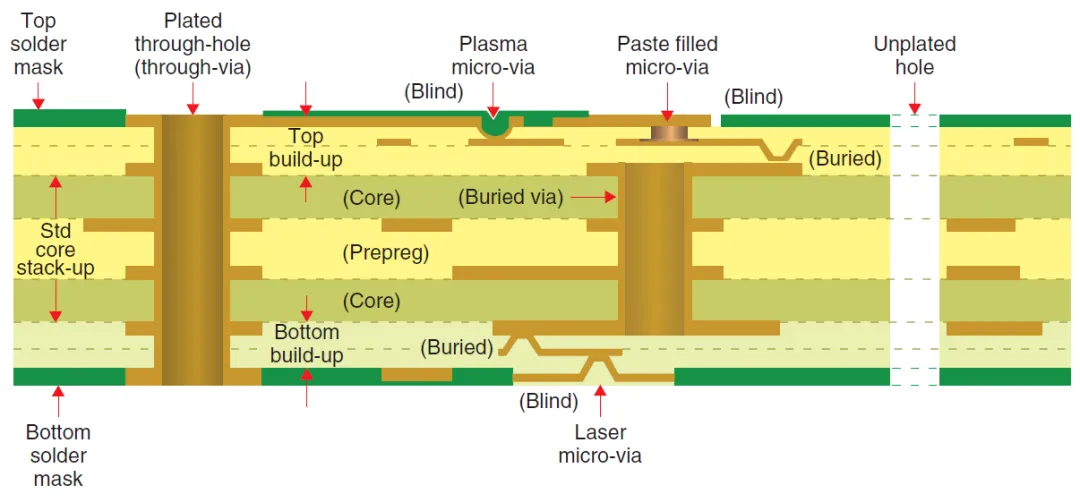
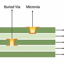
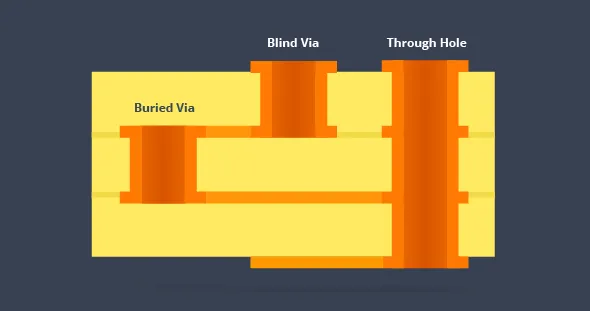
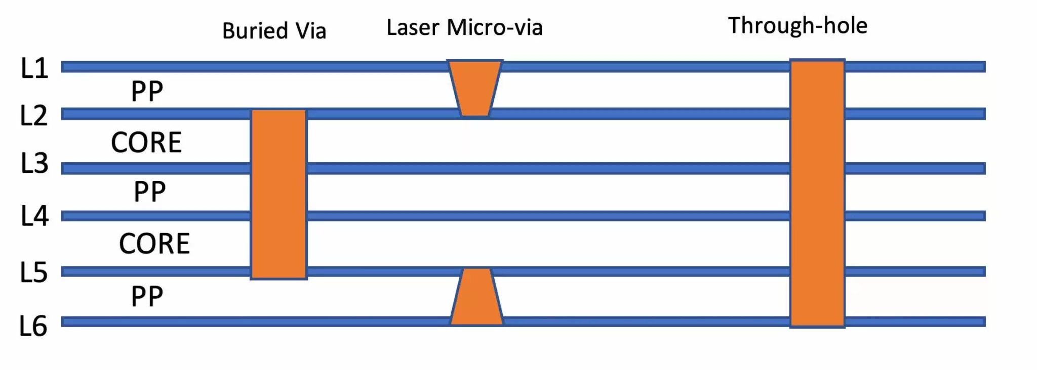
Buried vias are plated through-holes that interconnect two or more internal layers of a multilayer PCB, remaining completely hidden from the top and bottom surfaces. Unlike through-hole vias, which span the entire board thickness, buried vias enable finer pitch routing on surface layers by freeing up space otherwise occupied by unnecessary via stubs. This design choice matters in high-density interconnect applications where signal speeds demand controlled impedance paths and minimal crosstalk. In factory production, buried vias require precise core alignment during lamination to maintain electrical continuity and mechanical integrity. Electrical engineers appreciate their ability to support advanced architectures, but buried via cost analysis often shows elevated expenses from additional processing steps. Proper implementation aligns with industry standards to ensure long-term performance under thermal and mechanical stress.
Buried Via vs Through-Hole: Performance and Cost Trade-offs
Through-hole vias offer simplicity in fabrication, as they involve a single drilling and plating cycle across the full board stackup, keeping PCB fabrication costs low for standard designs. In contrast, buried vias necessitate multiple lamination cycles, where individual cores with pre-drilled vias are built up layer by layer, increasing handling time and yield risks. Performance-wise, buried vias excel in high-speed circuits by eliminating via stubs that introduce inductance and reflections in through-hole designs, making them preferable for RF and high-frequency applications. However, this comes at a premium in buried via cost analysis, as factories must invest in specialized alignment and inspection equipment to avoid misalignment defects. Engineers should compare via types based on board thickness and layer count; for example, in eight-layer boards, buried vias can reduce overall via count while through-holes suffice for power distribution. The key is selective use to avoid unnecessary cost escalation.
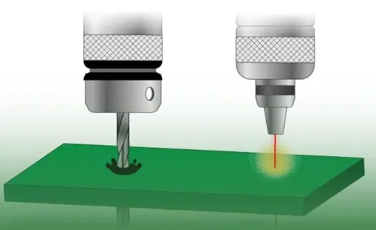
The Fabrication Process for Buried Vias and Its Cost Implications
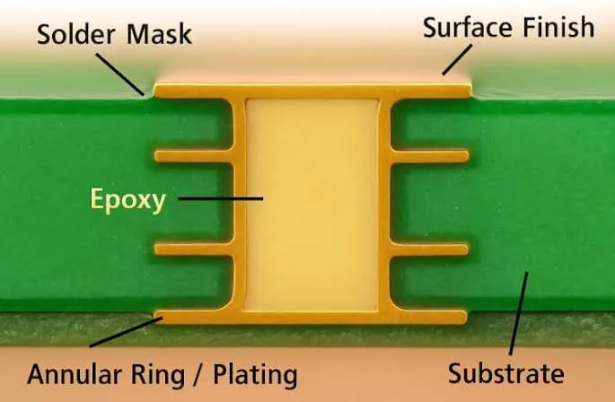
Fabricating buried vias begins with preparing individual cores, where vias are mechanically drilled or laser-ablated, then electroplated before lamination. Subsequent layers are added in a sequential build-up process, with photoresist imaging and etching to define traces around the buried structures. This multi-step approach heightens PCB fabrication costs through extended cycle times, increased material waste from yield losses, and rigorous quality checks like X-ray inspection for via fill integrity. Factories emphasize precise drill depth control to meet aspect ratio limits, as excessive ratios lead to plating voids that compromise reliability. Per IPC-4761 guidelines on via protection, options like filled or tented buried vias further influence costs, with filled types offering superior thermal performance but requiring additional epoxy or conductive paste dispensing. Engineers gain from understanding these steps to design for manufacturability, minimizing rework and expediting production.
Key Factors Driving Buried Via Costs
Several elements contribute to elevated costs in buried via implementation, starting with the number and size of vias specified in the design. Smaller diameters improve density but demand advanced drilling capabilities, raising setup fees and reducing throughput in the fabrication line. Layer count amplifies expenses, as more internal connections require additional lamination presses and alignment fiducials. Material selection, such as high-Tg laminates for stability during sequential buildup, adds to the baseline PCB fabrication costs. Yield variability poses another challenge, where misalignment or plating inconsistencies necessitate scrap and reprocessing. A thorough buried via cost analysis involves evaluating panel utilization, as buried via panels often yield fewer boards due to edge exclusion zones for process control.
Cost Reduction Strategies for Buried Via Implementation
To achieve cost-effective buried via usage, engineers should minimize their quantity by optimizing routing on inner layers and using them only where through-holes would impede surface traces. Staggering via locations across layers reduces alignment precision requirements, simplifying factory handling and cutting setup times. Selecting larger via diameters, where performance allows, enables standard mechanical drilling over laser methods, directly lowering PCB fabrication costs. Hybrid stackups combining buried vias in high-density regions with through-holes elsewhere balance density and expense effectively. Factories recommend panel-level design optimizations, like symmetric layouts to maximize usable area and reduce waste. Adhering to IPC-6012 performance specifications ensures first-pass yields, avoiding costly iterations while maintaining quality.
Another practical approach involves via-in-pad designs for buried structures, which consolidate connections and reduce overall via count, though plating uniformity must be verified. Collaborating early with fabrication partners on drill tables and stackup proposals uncovers opportunities for cost reduction strategies, such as shared tooling across production runs. Thermal management planning prevents warpage during lamination, preserving yield in multilayer builds. These tactics enable electrical engineers to implement buried vias without proportional cost increases.
Best Practices for Reliable and Economical Buried Via Designs
Designers should incorporate robust annular rings around buried vias to accommodate drill wander, as specified in IPC standards for plating reliability. Simulation tools help predict impedance mismatches early, justifying buried via placement only where signal integrity demands it. Factory-driven insights stress the importance of bake-out cycles post-lamination to remove moisture, preventing voids under reflow conditions. For cost reduction strategies, grouping buried vias in clusters facilitates efficient imaging and etching. Electrical testing protocols, including continuity checks on inner layers, confirm functionality before final assembly. These practices ensure buried vias deliver performance gains at minimized PCB fabrication costs. However, given the multi-step nature of buried via production, it is crucial to understand how PCB and assembly pricing is estimated to ensure your project stays within budget when using advanced fabrication methods.
Conclusion
Balancing performance and price in buried via implementation requires a deep understanding of fabrication challenges and strategic design choices. Buried via cost analysis underscores the need for selective use, hybrid via strategies, and manufacturability focus to control expenses. By leveraging larger vias, optimized stackups, and standard-compliant processes, electrical engineers can harness density benefits without excessive costs. Factory perspectives emphasize early planning and yield-focused designs for successful outcomes. Ultimately, these approaches enable innovative PCB solutions that meet tight budgets and high-performance requirements.
FAQs
Q1: What is buried via cost analysis, and why is it essential for PCB projects?
A1: Buried via cost analysis evaluates the added expenses from sequential lamination and inspection compared to simpler through-hole processes. It helps electrical engineers decide if density gains justify the premium, typically driven by via count and board complexity. Factories use this to quote accurately, factoring in yield risks. Strategic analysis prevents over-design, aligning costs with performance needs in multilayer boards.
Q2: How do buried via vs through-hole options impact PCB fabrication costs?
A2: Buried vias increase costs due to multiple build-up cycles, while through-holes use single-drill efficiency for lower prices. Through-holes suit power nets, but buried excel in signal layers for better integrity at higher expense. Engineers compare based on layer count; hybrids optimize both. This trade-off guides cost reduction strategies in high-density designs.
Q3: What are effective PCB cost reduction strategies for buried via designs?
A3: Key strategies include minimizing via numbers, using larger diameters for standard drilling, and symmetric panel layouts for better yields. Staggered placements ease alignment, and early stackup reviews uncover savings. Adhering to standards like IPC-4761 for protection reduces rework. These factory-aligned tactics lower fabrication costs while preserving performance.
Q4: When should engineers prioritize buried vias despite higher PCB fabrication costs?
A4: Prioritize buried vias in high-speed, dense boards where stub inductance from through-holes degrades signals. They enable finer routing without surface clutter, ideal for RF modules. Cost analysis confirms value when layer savings offset fab premiums. Factory processes support this for applications demanding superior integrity.
References
- IPC-4761 — Via Protection Guidelines for Printed Boards. IPC, 2020
- IPC-6012E — Qualification and Performance Specification for Rigid Printed Boards. IPC, 2017
- IPC-A-600K — Acceptability of Printed Boards. IPC, 2020