










Everyday PCB design is a compromise among signal integrity, impedance control, routing density, design complexity, and manufacturing cost. Designers working with six-layer boards often discover that a conventional 1.6 mm stackup forces outer-layer and inner-layer traces to be wider than the layout can comfortably support. That width penalty becomes especially painful around small-package BGAs and dense high-speed differential pairs. A practical stackup technique that is easy to overlook in this situation is the pseudo eight-layer structure.
A pseudo eight-layer board is still physically a six-layer construction. By changing how cores and prepregs are stacked, and by inserting a no-copper core in the center of the board, the stackup can behave more like an eight-layer board in material arrangement and electrical performance. The result is narrower controlled-impedance traces without moving to a full eight-layer process.
What Is a Pseudo Eight-Layer?
In some six-layer designs, engineers adopt a special stackup that, although physically six layers, behaves similarly to an eight-layer board in terms of material stacking and functional performance. The industry calls this approach a "pseudo eight-layer."
01 | PCB Stackup Fundamentals
A multilayer PCB is built from a small set of materials that together determine thickness, dielectric spacing, and copper geometry.
- Core: a rigid dielectric substrate with copper foil on one or both sides. Cores form the dimensional backbone of the board and set several of the inner-layer dielectric thicknesses.
- Prepreg (PP): a partially cured bonding sheet placed between cores or between a core and an outer copper foil. During lamination the resin flows, fills spaces around traces, and then cures, locking the stack together.
- Solder mask: the outer protective coating that covers copper, prevents solder bridging, and also forms part of the outer-layer dielectric environment used in impedance calculations.
Layer-to-layer spacing is not an independent drawing dimension. It is the combined result of core thickness, prepreg thickness after flow and cure, copper thickness, and residual resin. Those distances, together with trace width and copper weight, are what set characteristic impedance. Changing only the schematic layer count does not automatically fix an impedance or density problem if the dielectric thicknesses stay the same.
02 | What Is Impedance Control?
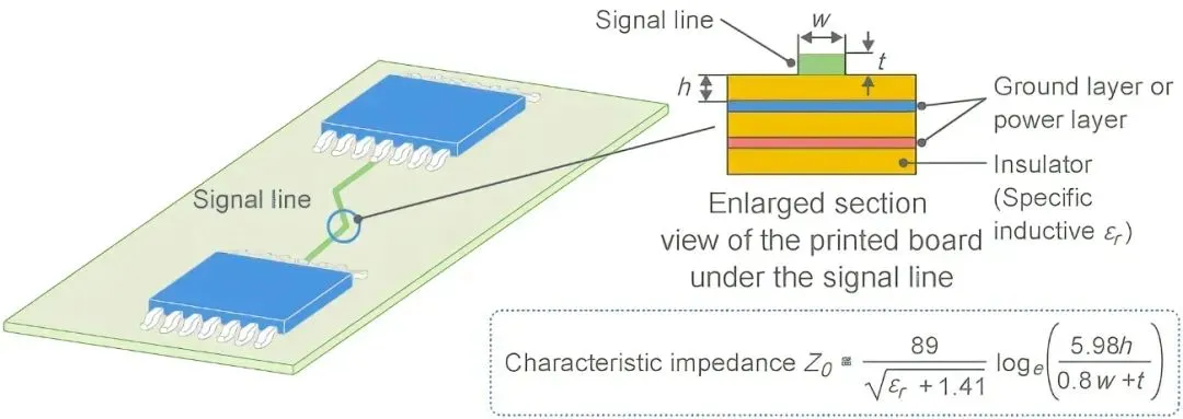
In high-speed designs, impedance matching is a primary factor in signal quality. When the characteristic impedance of a trace does not match the driver, receiver, or interconnect target, part of the traveling wave reflects. Reflections produce overshoot, undershoot, ringing, and waveform distortion. In severe cases they close timing and voltage margins enough to cause functional failures.
The impedance of a given trace depends on several stackup and geometry variables at once:
- Board material type and dielectric constant
- Dielectric thickness between the signal layer and its reference plane
- Trace width, trace spacing, and copper thickness
- Whether solder mask is present over the trace
For a target single-ended or differential impedance, a thicker dielectric generally requires a wider trace. That relationship is why a conventional thick six-layer stackup often produces traces that are electrically correct but physically too wide for dense routing.
Back to the Point: Why Does a Six-Layer Board Sometimes Fall Short?
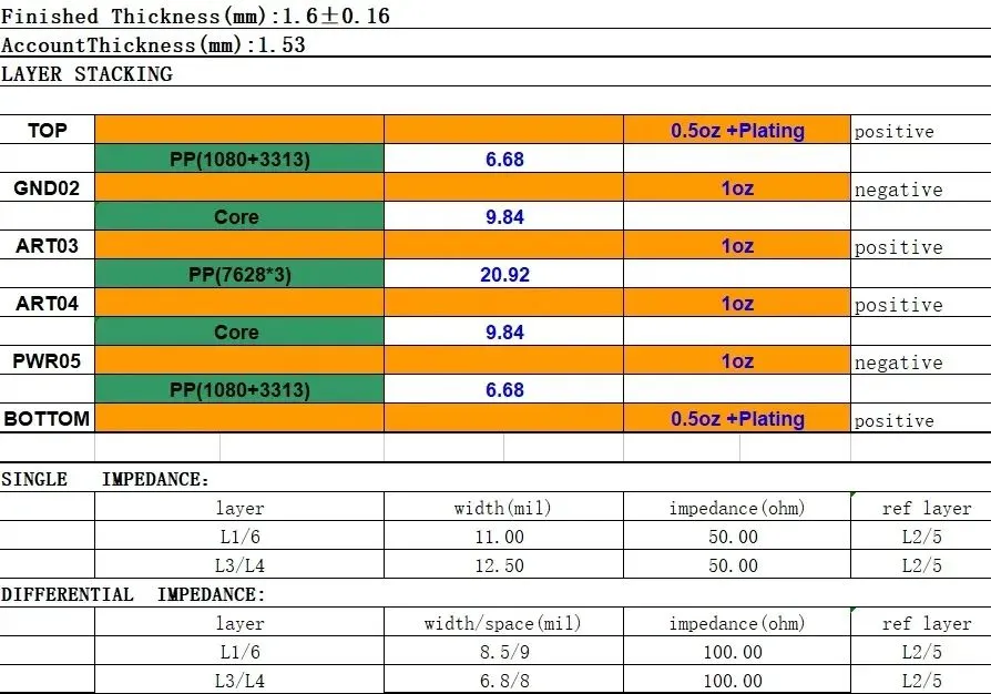
On a conventional 1.6 mm six-layer stackup, outer-layer and inner-layer traces used for controlled impedance frequently become large enough to reduce routing density. Typical geometry that appears in this class of stackup includes:
- Single-ended 50 Ω trace width of about 11 mil
- Differential 100 Ω trace width and spacing of about 8.5 mil / 9 mil
- Inner-layer traces that may need to be as wide as 12.5 mil
Those widths leave little room between balls of a fine-pitch BGA, reduce the number of signals that can escape a congested channel, and make it harder to keep differential pairs tightly coupled while still meeting spacing rules to neighboring nets. The electrical target may be met, but the layout becomes harder than the layer count suggests it should be.
The root cause is dielectric thickness. If surface prepreg and core thicknesses remain relatively large in order to build a 1.6 mm finished board with only six copper layers, the designer is forced to widen traces to hold 50 Ω or 100 Ω. Adding layers would allow thinner dielectrics and narrower traces, but a full eight-layer board increases material, lamination, and drilling cost. The pseudo eight-layer approach is an attempt to recover some of that electrical geometry without paying the full eight-layer premium.
Solution: The Pseudo Eight-Layer Stackup
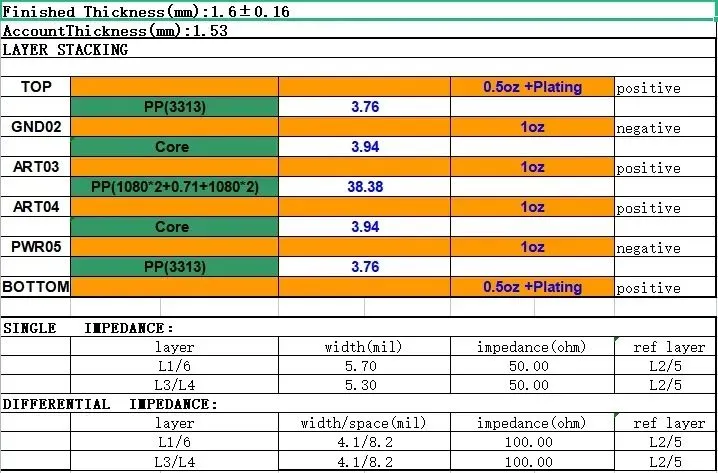
The method is to optimize the stackup by thinning the surface prepreg and the cores that set signal-to-plane spacing, then adding a no-copper core in the central region of the board. The no-copper core contributes finished thickness so the board can still meet a 1.6 mm class target, while the signal-related dielectrics stay thin enough to support narrower traces.
Because the central core has no copper, it does not introduce additional signal or plane layers and does not create extra impedance discontinuities in the signal path. Its job is mechanical and dimensional: increase overall thickness without placing extra copper close to the high-speed layers. That arrangement also helps avoid an overly thick interlayer resin fill in the middle of the stack, which can increase the risk of layer shifting during lamination.
With this type of stackup, controlled-impedance geometries can be reduced to approximately:
- Outer-layer single-ended trace width of 5.7 mil
- Differential trace width and spacing of 4.1 mil / 8.2 mil
- Inner-layer trace width of 5.3 mil
Those values are a substantial improvement over the 11 mil, 8.5 mil / 9 mil, and 12.5 mil geometries associated with a conventional 1.6 mm six-layer stackup. For layouts that are already routing-limited, the narrower traces free escape channels, ease pair spacing, and make impedance-controlled routing more compatible with small packages.
Advantages of the Pseudo Eight-Layer
Narrower traces for high-density routing
Thinner surface prepreg and thinner signal-related cores lower the dielectric height used in the impedance calculation. The same 50 Ω or 100 Ω target can therefore be met with a smaller trace width. That change is what enables controlled impedance on small-package devices and on high-speed differential routes that would otherwise consume too much channel width.
Lower coupling between adjacent inner layers
Placing additional thickness between layer 3 and layer 4 increases the separation of those two routing layers. Greater distance reduces electric and magnetic coupling, which lowers crosstalk and improves signal quality when both layers carry active nets. The benefit is strongest when the two layers are not used as a tightly coupled broadside pair.
Cost that sits between six and eight layers
The construction remains a six-layer copper process with an extra no-copper core. Material and process cost is therefore typically higher than a standard six-layer board but lower than a full eight-layer board. For designs that need eight-layer-like trace widths and layer separation, but do not need two extra copper layers for power or additional routing, the cost-performance balance can be attractive.
Design Precautions
The core idea is the added no-copper core. Used correctly, it builds finished thickness without forcing an excessively thick resin-rich region between copper layers, which is one contributor to layer-to-layer shift during lamination. The no-copper core should be treated as a thickness and process element, not as a hidden routing layer.
When both layer 3 and layer 4 are used for routing, the preferred practice is orthogonal routing—for example, layer 3 horizontal and layer 4 vertical. Orthogonal directions keep parallel run length short and reduce broadside coupling that would otherwise offset some of the crosstalk benefit gained from the extra separation.
Impedance still depends on material type, dielectric constant, finished dielectric thickness, copper thickness, and solder mask. Thinning prepreg and core does not remove the need to calculate or simulate impedance with the actual stackup. The 5.7 mil, 4.1 mil / 8.2 mil, and 5.3 mil geometries described here belong to this stackup approach; they should not be copied onto a conventional thick six-layer construction and expected to hit the same impedance.
Designers should also keep fabrication constraints in view. Narrower traces and thinner dielectrics increase the importance of etch compensation, registration, and dielectric thickness control. The stackup only delivers its density and signal-quality benefit if the fabricated thicknesses stay close to the values used for impedance design.
Used with those constraints in mind, a pseudo eight-layer stackup is a targeted way to recover routing density and impedance geometry on a six-layer board: thinner signal dielectrics for narrower traces, a no-copper center core for finished thickness and inner-layer separation, and a cost position between a standard six-layer board and a full eight-layer board.






