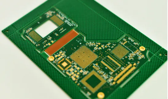
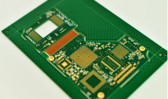
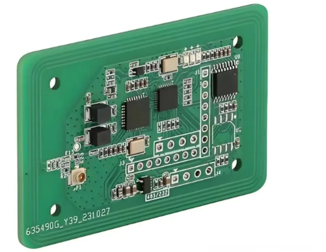
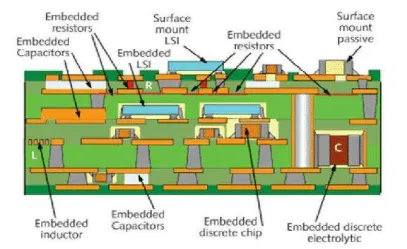
Phones, notebooks, and high-end industrial equipment keep getting thinner while performance rises. The component count inside the product does not disappear. The extra density often comes from an advanced PCB process: embedded resistors and embedded capacitors.
In this process, resistors and capacitors that would normally be mounted on the board surface are placed inside inner layers of the PCB. This article explains what the process is, how it differs from surface-mount assembly, and where its limits are.
What Embedded R and C Are, and How They Differ From Conventional Assembly
On a conventional PCB, resistors and capacitors are soldered on the surface as SMT parts. They occupy board area and are more exposed to external interference.
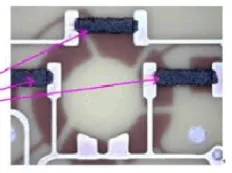
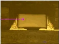
In the embedded-resistor and embedded-capacitor process, the parts are placed in inner layers. The board uses a dedicated structure. From bottom to top the described stack is: first dielectric layer, embedded resistor, circuit layer, and second dielectric layer. On the portion of the embedded resistor that is not covered by the circuit layer, a dedicated polymer isolation layer is applied so process chemicals cannot attack the resistor. That isolation layer is a key reason the construction can be produced in volume.
In short, the conventional process mounts parts on the surface. The embedded process places them inside the board. That change is what produces the density and electrical differences below.
Advantages
The process is used on high-end electronics because it addresses several layout and electrical constraints.
1. Board Area
With resistors and capacitors inside the stackup, the surface no longer has to carry a dense field of SMT passives. That frees area so a more complex circuit can fit on a smaller board. It is one reason phones and smartwatches can be made smaller.
2. Noise
Surface-mount passives are more exposed to electromagnetic interference, which can add circuit noise. Embedded resistors and capacitors are enclosed by the laminate, so interference is reduced and the circuit can run more stably.
3. Signal Path
Embedding the parts shortens the signal path and reduces delay and reflection loss. Signal integrity and reliability improve. That matters on phones, base stations, and high-end industrial equipment with tight signal requirements.
4. Thickness
Fewer surface parts allow a thinner PCB. With thin embedded-capacitor cores and other dedicated materials, the board can be thinner and lighter, which matches the trend toward slimmer products.
Process Steps
Embedding a part is not a simple insertion. The manufacturing flow has four steps, each with tight process limits.
Step 1: Build a Dedicated Inner Layer
In addition to the usual outer and inner layers, a separate inner layer is made for the embedded resistors and capacitors, with reserved areas for those parts. Plating and etching used in conventional PCB fabrication are applied so the layer stays within tolerance.
Step 2: Use a Special Package
A standard resistor or capacitor cannot be buried as-is. It must be packaged in a thin form that matches PCB thickness and has adequate thermal conductivity so heat during operation does not degrade performance.
Step 3: Place the Parts in the Layer
This is the core step. Two methods are used: press the packaged resistor or capacitor into the inner-layer material with a dedicated lamination process, or laser-machine a cavity in the inner-layer material and fill the part into that cavity. Both methods require high placement accuracy.
Step 4: Laminate and Interconnect
The inner layer that already contains the parts is then joined to the other conventional layers by lamination and drilling to form a complete board, with continuous connections between layers.
Limits
The process is not universal. Two limits explain why it is still used mainly on high-end products:
- Fabrication and repair are more difficult. The resistor or capacitor is inside the board and cannot be inspected directly. It cannot be replaced like an SMT part. Repair is hard, and a failure can scrap the whole board.
- Cost is higher. Special packages, a precise embedding flow, and dedicated materials make an embedded-R/C board more expensive than a conventional PCB.
For those reasons the process is used where performance, area, and thickness are tightly constrained: flagship phones, high-end servers, precision industrial equipment, and aerospace electronics.
Summary
Embedded resistors and capacitors are a PCB process built for high density, high performance, and thin constructions. Placing the passives inside the board reduces the area, interference, and thickness limits of surface-mount assembly and supports smaller, higher-performance products.
As process cost falls and accuracy improves, the method may move from high-end products into a wider set of commercial electronics that need small size and high performance together.