










During the CAM review of a 2-layer FR-4 board measuring 161.5 mm by 177.5 mm, our engineering team observed multiple silkscreen characters placed directly on component pads. From a DFM perspective, this created an immediate risk to solder joint quality. The primary concern was manufacturing stability during assembly rather than simple fabrication feasibility. Without clarification, the white legend ink could remain on the pad surfaces after solder-mask processing and interfere with lead-free HASL wetting, leading to incomplete solder joints or cosmetic rejects.
The order specified TG150 material, 1.6 mm thickness, 1 oz copper on both sides, green solder mask on both sides, white silkscreen, customer self-panelization with scoring separation, no process edge, and a one-day delivery window. Quantity was 30 pieces in 15 sets. These parameters are typical for a compact 2-layer design, yet the combination of silkscreen overlapping pads and an ambiguous half-hole feature required explicit engineering confirmation before the files could be released.
Why Silkscreen Placement on Pads Triggered Immediate DFM Scrutiny
Our CAM engineer began by comparing the silkscreen layer against the copper and solder-mask openings. Multiple text characters sat fully or partially inside pad areas. In a standard process the white legend is applied after solder mask and before surface finish. Any ink that remains on a pad surface after curing can act as a physical barrier to solder wetting during assembly.
At the same time the design contained arrow-marked half-hole features, yet the order ( #FR4-20260403-027 ) form did not state whether these should be processed as plated castellation holes or as non-plated holes. The team therefore recorded both observations and prepared a single Engineering Question that prioritized the silkscreen-on-pad risk because of its direct impact on solderability.
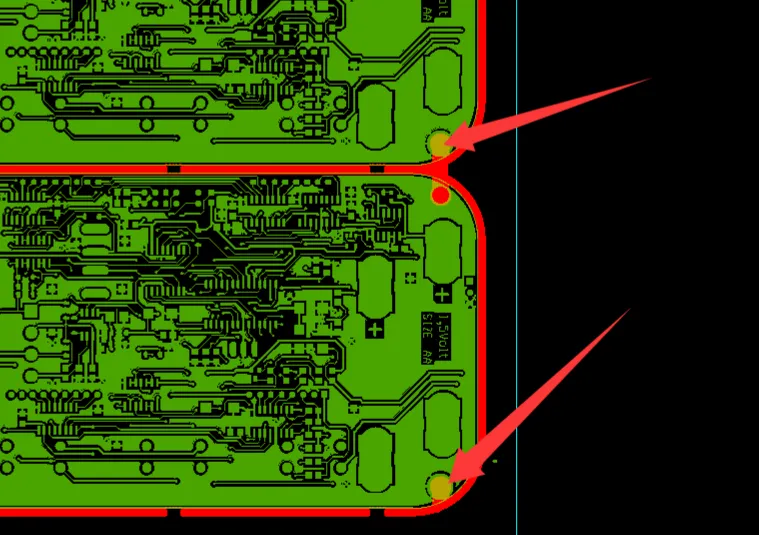
Figure 1: half-hole (castellated hole) at the location indicated by the arrow
Risk indicators included the dense placement of legend characters relative to the 0.3 mm hole size, the use of scoring without a process edge, and the short one-day lead time that left little margin for post-fabrication rework. On a green-mask board with white silkscreen the contrast makes residual ink highly visible, increasing the chance of visual rejects even if electrical performance is only marginally affected.
| Observed Feature | Condition in Files | Primary DFM Risk |
|---|---|---|
| Silkscreen characters | Multiple locations on pads | Solder wetting interference |
| Half-hole features | Present but unspecified | Ambiguous plating requirement |
| Panel construction | Customer scoring, no edge | Limited rework flexibility |
Silkscreen on Pads and Half-Hole Ambiguity as Core Manufacturability Risks
The dominant risk was residual silkscreen ink on pad surfaces. When white legend remains inside a solder-mask opening, it can prevent complete coverage by the lead-free HASL finish or create a non-wetting zone during reflow. The secondary risk was the undefined castellated hole treatment. Leaving the feature as designed without clarification could result in either unintended plating or missing copper on the board edge, both of which affect edge connector reliability.
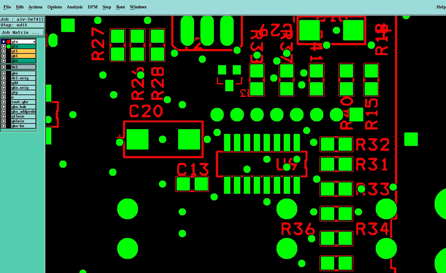
there are many characters designed on the pads
A third, lower-severity observation concerned the overall panelization. With customer-supplied scoring and zero process edge, any post-fabrication correction of silkscreen defects would be difficult and time-consuming, especially under a one-day delivery constraint.
From a DFM perspective these issues formed a clear priority sequence: remove or relocate the characters on pads first, then lock the half-hole process definition, and finally confirm the panel handling rules. Ignoring the silkscreen overlap would have the highest probability of generating assembly-related rejects.
How Residual Legend Ink Compromises Solder Joint Integrity
If production had continued without removing the characters from the pads, the white silkscreen ink would have cured on the copper surfaces. During the subsequent lead-free HASL process the ink acts as a mask, limiting solder coverage. The resulting pad may show partial wetting or a dark residue that fails visual inspection under IPC-A-600 criteria for surface finish coverage.
At assembly the same residual ink can produce incomplete solder fillets, tombstoning of small components, or open joints that only appear after thermal cycling. On a 2-layer board with relatively large pads the defect rate can rise quickly because the ink coverage is continuous rather than a small intrusion.
For the half-hole features, processing them as plated castellation without customer intent could leave unwanted copper on the board edge, while treating them as non-plated holes without confirmation could remove intended edge conductivity. Either outcome creates a mismatch between the fabricated board and the intended mating connector.
| Failure Mode | Linked to EQ Item | Production or Field Impact |
|---|---|---|
| Incomplete solder wetting | Silkscreen characters on pads | Assembly rejects, rework |
| Visual surface-finish defects | Residual legend ink | Scrap under IPC-A-600 |
| Edge connector mismatch | Undefined half-hole plating | Mating or continuity failure |
| Limited rework window | One-day delivery + scoring | Delayed shipment if defects found |
Failure Scenarios Avoided by Prompt Engineering Confirmation
Had the silkscreen characters remained on the pads, boards reaching the assembly line would have shown incomplete HASL coverage on those pads. Operators would then face a choice between accepting reduced solderability or attempting manual cleaning, both of which increase cost and cycle time. In a worst realistic case the residual ink could cause intermittent opens after temperature cycling, generating field returns that are difficult to attribute to the original legend design.
Leaving the half-hole definition unresolved could have produced boards whose edge features did not match the mating connector drawing. The resulting continuity failures would appear only after final system integration, forcing a complete panel respin under an already aggressive one-day schedule.
Because the panel used scoring and carried no process edge, any post-fabrication correction of either defect would have required individual board handling and risked additional edge damage. Early confirmation therefore protected both yield and the short delivery commitment.
Preventive Actions Confirmed with the Customer
Our engineering team issued a concise Engineering Question that first recommended removing all characters located on pads so that solder-mask openings would remain free of legend ink. The customer accepted the recommendation with the explicit statement "Accept removing characters on pads." This single decision eliminated the primary solderability risk.
For the half-hole features the team proposed treating them as non-plated holes (NPTH) unless the customer required plated castellation. The customer confirmed fabrication as NPTH, removing ambiguity from the edge processing sequence.
File confirmation closed the loop. With both answers in hand the CAM data were updated: silkscreen characters overlapping pads were deleted, half-hole locations were coded as NPTH, and the panel was released under the agreed one-day schedule. The revised files retained all functional copper and soldermask features while restoring clean pad surfaces for reliable HASL and subsequent soldering.
| Action Item | Customer Response | Manufacturing Outcome |
|---|---|---|
| Remove characters on pads | Accepted | Clean pad surfaces for HASL and soldering |
| Half-hole processing | Fabricate as NPTH | Consistent edge definition |
| Overall file release | Confirmed | On-time production under 1-day window |
Building Trust Through Early Legend and Edge Clarification
This case demonstrates that silkscreen characters placed on pads are not a minor cosmetic detail; they constitute a direct threat to solder joint formation and final inspection yield. By identifying the overlap during CAM review and obtaining explicit customer approval to remove the characters, the engineering team protected both the one-day delivery commitment and the long-term reliability of the assembled boards.
Designers working with white silkscreen on green-mask 2-layer boards are encouraged to keep all legend text outside solder-mask openings and to declare half-hole requirements clearly on the fabrication drawing. When these two points are verified early, the risk of assembly defects and edge mismatches drops dramatically. Proactive DFM confirmation remains the most effective way to turn potential manufacturing problems into controlled, documented decisions before production begins.
FAQ
Q1: Why does silkscreen on pads create a soldering risk?
A1: The cured legend ink forms a non-wettable barrier on the copper surface. During lead-free HASL or subsequent reflow the solder cannot fully wet the pad, producing incomplete fillets, voids, or open joints that may escape electrical test yet fail under thermal stress.
Q2: What happens if residual silkscreen ink is left on pads after fabrication?
A2: Visual inspection under IPC-A-600 may reject the boards for incomplete surface-finish coverage. At assembly the same ink can cause tombstoning or intermittent opens, generating rework or scrap that is far more expensive than a simple CAM edit.
Q3: Why must half-hole features be explicitly defined on the order?
A3: Half-holes can be processed as plated castellation or as non-plated holes. Without a clear statement the factory may apply the wrong copper and plating sequence, resulting in edge features that do not match the intended connector and causing continuity failures after system integration.
Q4: How does a short delivery window increase the importance of early DFM checks?
A4: With only one day available there is almost no margin for post-fabrication correction. Identifying and resolving silkscreen-on-pad and half-hole issues before tooling release protects both yield and the committed ship date.
Q5: Can silkscreen characters be safely placed near pads if they do not overlap?
A5: Yes, provided a minimum clearance is maintained so that registration tolerance cannot push the ink into the solder-mask opening. When characters sit fully or partially inside the pad, removal is the safest preventive action.
Q6: How can designers avoid similar Engineering Questions on future 2-layer boards?
A6: Keep all silkscreen text outside solder-mask openings, declare half-hole plating requirements explicitly on the fab drawing, and request a DFM review of the legend layer before final release. These steps convert potential assembly risks into controlled design decisions.






