Introduction
Polyimide PCBs represent a cornerstone in flexible electronics manufacturing, offering exceptional thermal stability and mechanical flexibility for demanding applications. Electric engineers often turn to polyimide substrates in the PCB manufacturing process due to their ability to withstand extreme temperatures and repeated bending cycles. This guide walks through the polyimide PCB fabrication journey from initial concept to functional prototype, emphasizing key stages in flex PCB prototype development. Understanding these steps ensures reliable performance in electronic manufacturing environments like aerospace and medical devices. By following factory-driven protocols, engineers can minimize defects and accelerate prototyping timelines. The process demands precision to leverage polyimide's inherent properties while adhering to established quality benchmarks.
What Are Polyimide PCBs and Why They Matter in Prototyping
Polyimide PCBs utilize polyimide films as the base dielectric material, typically laminated with copper foil to form flexible circuits. These boards excel in high-temperature environments, with glass transition temperatures often exceeding 250 degrees Celsius, making them ideal for applications where rigid FR-4 substrates fail. In the context of prototype fabrication of flex PCBs, polyimide enables compact designs that conform to irregular shapes, reducing assembly complexity in space-constrained systems. Factory insights reveal that polyimide's low moisture absorption and chemical resistance enhance long-term reliability under vibration and thermal cycling. IPC-4202 specifies requirements for flexible base dielectrics like polyimide, ensuring consistent electrical and mechanical properties across production runs. For electric engineers prototyping high-reliability electronics, selecting polyimide streamlines the transition from design to volume manufacturing.
Step 1: Conceptual Design and Material Selection
The journey begins with translating engineering requirements into a manufacturable design, focusing on circuit layout, bend radii, and layer stack-up. Engineers must specify copper thickness, typically 1 oz/ft2 or 1/2 oz/ft2 for fine-pitch traces in polyimide PCB fabrication. Adhesiveless polyimide-copper laminates are preferred for prototypes to avoid delamination risks during flexing. Material selection considers polyimide thickness, often 25 to 50 microns, balanced against signal integrity needs. Design files should include bend areas with strain-relief features to prevent cracking. This phase sets the foundation for efficient electronic manufacturing by aligning with fabrication capabilities.
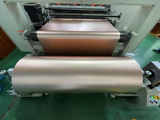
Step 2: Substrate Preparation and Pre-Treatment
Raw polyimide film arrives with copper cladding, requiring careful handling to prevent contamination. Pre-baking in a convection oven removes absorbed moisture, a critical step since polyimide is hygroscopic and can cause voids during lamination. Panels undergo surface cleaning via chemical desmear or plasma treatment to ensure adhesion of subsequent layers. Factory protocols emphasize controlled humidity below 50% during storage and processing. Edge beveling prepares panels for precise registration in imaging equipment. Proper preparation minimizes defects in the flex PCB prototype, enabling smooth progression through imaging.
Step 3: Circuit Patterning via Photolithography and Etching
Dry film photoresist laminates onto the copper surface under heat and pressure, followed by UV exposure through a phototool. Development reveals the circuit pattern, exposing copper areas for etching. Chemical etching removes unwanted copper using ferric chloride or cupric solutions, forming precise traces with controlled linewidths. Post-etch stripping cleans the panel, inspecting for undercuts or bridging per visual standards. For prototypes, tenting techniques protect fine features during etching. This stage defines the PCB manufacturing process's core, where tolerances below 75 microns become feasible with polyimide's stability.
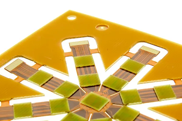
Step 4: Coverlay Application for Insulation
Coverlay, a polyimide film with adhesive, applies to protect traces and enable flexing. Alignment ensures precise cutouts for pads and vias, laminated under vacuum to eliminate air pockets. Curing bonds the coverlay, followed by laser or mechanical routing for exposure. Factory-driven best practices include pre-curing adhesive to control flow during lamination. This insulation layer enhances environmental resistance in electronic manufacturing. For single-sided flex prototypes, coverlay completes the basic structure ready for interconnection features.
Step 5: Multilayer Build-Up and Lamination
Multilayer polyimide PCBs assemble by aligning etched cores with coverlays or bonding films. Sequential lamination presses layers at elevated temperatures, fusing adhesives without degrading polyimide integrity. Registration holes maintain layer-to-layer alignment within 50 microns. Blind or buried vias form through controlled drilling post-lamination. This process suits complex flex PCB prototypes requiring signal routing across bends. Engineers benefit from iterative stack-up simulations to predict warpage.
Step 6: Via Formation, Plating, and Interconnection
Laser drilling creates microvias in polyimide, followed by desmear to expose copper pads. Electroless copper seeds vias, with electrolytic plating building conductive barrels. Flash plating minimizes buildup on surfaces while filling vias reliably. IPC-6013 outlines qualification criteria for these interconnections, ensuring performance in flexible boards. Prototype runs prioritize filled vias for planar surfaces in subsequent assembly. This step integrates rigid-flex transitions if hybrid designs are prototyped.
Step 7: Surface Finishing, Stiffeners, and Outline
Electrolytic or immersion finishes like ENIG or OSP apply to exposed pads for solderability. Polyimide or FR-4 stiffeners attach via adhesive or lamination at connector or component sites. Mechanical or laser routing outlines the panel into individual circuits, incorporating scored lines for easy separation. Solder mask over bare copper areas adds protection where needed. Factory quality checks verify flatness and adhesion. These finishes prepare the flex PCB prototype for PCB assembly guide integration.
Step 8: Electrical Testing and Qualification
Flying probe or bed-of-nails testers verify continuity and shorts on the completed prototype. Flex-specific tests include cyclic bending per IPC standards to simulate operational stresses. Thermal shock and humidity exposure assess reliability. Visual and automated optical inspection detect anomalies like coverlay bubbles. Data logging supports design iterations for electric engineers. Passing these ensures the polyimide PCB fabrication yields production-viable prototypes.
Best Practices for Polyimide Flex PCB Prototype Production
Prototype fabrication favors adhesiveless laminates to reduce thermal expansion mismatches. Limit layer counts to four for quick turnaround in electronic manufacturing. Specify minimum bend radii at 10 times copper thickness to avoid fatigue. Collaborate with fabricators early on panel utilization to optimize costs. IPC-2223 provides design guidelines preventing common pitfalls like trace cracking. Document all process parameters for repeatability in scaling to production.
Conclusion
Mastering the polyimide flexible PCB manufacturing from concept to prototype empowers electric engineers to innovate in flexible electronics. Each step, from substrate prep to qualification, builds reliability into the flex PCB prototype. Adhering to standards ensures consistency across batches. This guide equips teams for efficient electronic manufacturing, bridging design intent with functional hardware. Future prototypes will leverage these insights for even tighter integrations.
FAQs
Q1: What are the key differences in the PCB manufacturing process for polyimide versus rigid boards?
A1: Polyimide PCB fabrication emphasizes moisture control and adhesiveless bonding to handle flexibility, unlike rigid processes focused on drilling thick FR-4. Lamination uses lower pressures to preserve bend properties. Laser vias replace mechanical drilling for precision. Factory protocols prioritize coverlay over solder mask for insulation. This suits flex PCB prototype needs in high-temp apps. Overall, polyimide demands specialized handling for superior dynamic performance.
Q2: How does IPC-6013 influence polyimide PCB fabrication quality?
A2: IPC-6013 sets qualification specs for flexible boards, mandating tests for adhesion, continuity, and flex endurance. It guides via plating and lamination integrity in prototypes. Engineers use it to verify warpage limits post-processing. Compliance reduces field failures in electronic manufacturing. Factories align processes to its class levels for prototypes. This standard ensures prototypes mirror production reliability.
Q3: What role does pre-baking play in flex PCB prototype fabrication?
A3: Pre-baking removes moisture from polyimide films, preventing voids and delamination during lamination. It typically occurs at controlled temperatures before imaging. This step enhances copper adhesion and trace yield. Neglect risks bow in multilayer builds. Best for humid environments in PCB manufacturing process. Electric engineers specify bake times based on film thickness.
Q4: Can polyimide PCBs handle PCB assembly guide requirements for high-volume production?
A4: Yes, polyimide supports standard SMT processes with proper stiffening for pick-and-place. Its thermal stability aids reflow soldering without warping. Prototypes test assembly compatibility early. Coverlay protects traces during handling. This aligns with electronic manufacturing scalability. Engineers validate via assembly trials.
References
IPC-6013E — Qualification and Performance Specification for Flexible and Rigid-Flex Printed Boards. IPC, 2020
IPC-4202B — Flexible Base Dielectrics for Use in Flexible Printed Circuitry. IPC, 2015
IPC-2223C — Sectional Design Standard for Flexible/Rigid-Flexible Printed Boards. IPC, 2019