 00:51
00:51
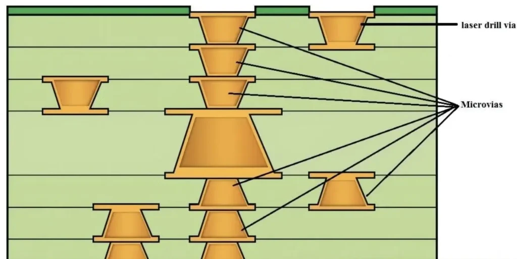
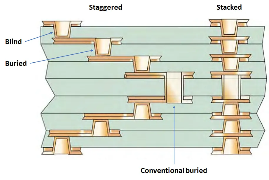
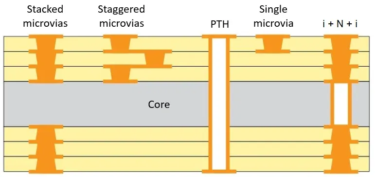
PCB Vias
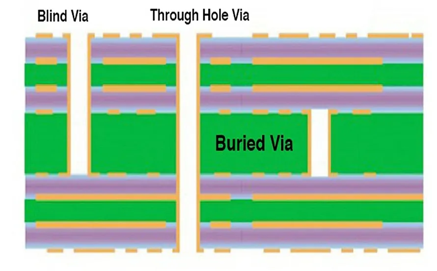
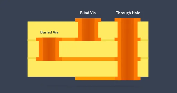
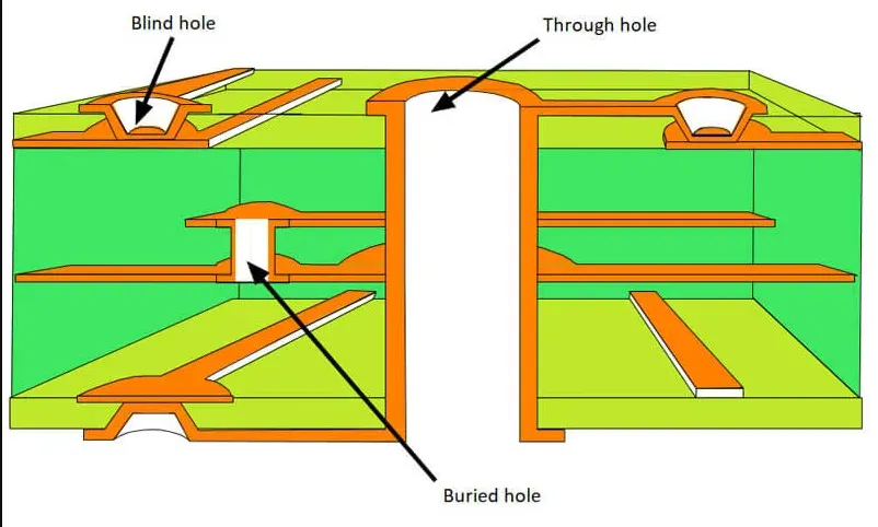
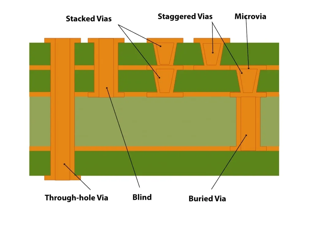
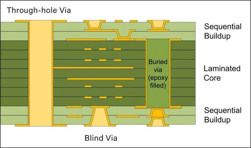
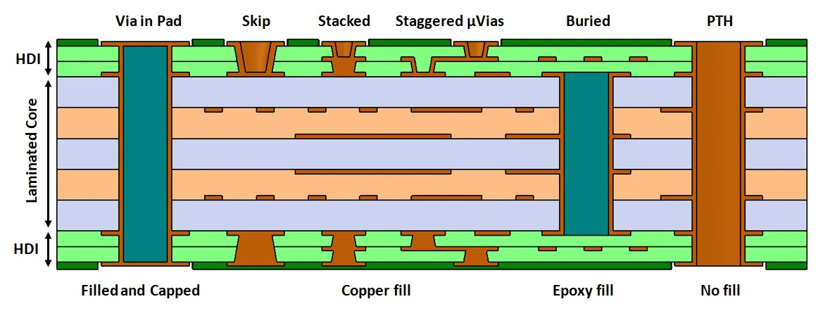
PCB vias are essential components in printed circuit board design, serving as conductive pathways that connect different layers of a multilayer PCB. These small plated holes enable electrical signals to travel vertically through the board, allowing for more compact and efficient layouts compared to single-layer designs. For engineers and hobbyists searching for information on PCB vias, this tag aggregates a wealth of resources that delve into their fundamental principles, helping you understand how they facilitate signal integrity, thermal management, and overall board performance in complex electronic systems. In practical terms, PCB vias come in various types, including through-hole vias that span the entire board, blind vias that connect an outer layer to an inner one without penetrating fully, and buried vias that link internal layers only. Each type offers specific advantages depending on your project's requirements, such as minimizing signal interference in high-speed circuits or optimizing space in densely populated boards. By exploring the articles under this tag, you can gain actionable insights into selecting the right via type for applications like RF designs, power electronics, or automotive systems, where reliability is paramount. Best practices for implementing PCB vias include adhering to design rules that prevent issues like via tenting, annular ring violations, or excessive thermal stress during soldering. For instance, ensuring proper via sizing and placement can reduce impedance mismatches and improve manufacturability, ultimately leading to fewer prototypes and faster time-to-market. Whether you're troubleshooting common problems like via voids or seeking tips on via stitching for ground planes, the content here provides detailed guidance grounded in industry standards. Diving into these articles will equip you with the knowledge to enhance your PCB designs, from basic concepts to advanced techniques, ensuring your projects meet both functional and production demands.
Video Guide
-
00:51
-
 00:57
00:57
PCB Solder Mask: Essential Protective Layer in Manufacturing
-
 00:54
00:54
PCB Vias: Critical Design Factors for Manufacturing Yield and Reliability
-
 00:57
00:57
PCB Antipad Design: 4 Key Factors for Reliable High-Speed Multilayer PCBs
-
 00:59
00:59
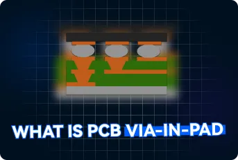
Via-in-Pad for BGA PCBs: When to Use It and Critical DFM Rules
-
 00:57
00:57
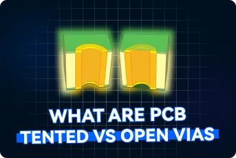
Tented vs Untented Vias — Why It Matters for Reliability
-
 01:09
01:09
How Signals Jump Between PCB Layers: Vias Explained
Technical Articles
HDI PCB Design: Overcoming Challenges in High-Density Interconnect
The Art of Blind and Buried Vias in High-Density Ultrasound PCBs
Mastering Hand-Soldering on Blind Via PCBs: A Hobbyist's Guide
PCB CAM Review: Fix V-Cut & Via Spacing to Avoid Delays
Via Design and Its Effect on PCB Signal Integrity: Optimization Strategies
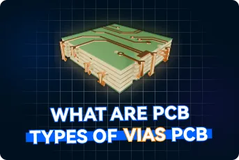
Via Technology in PCB Manufacturing: Types, Design Rules, and Optimization Techniques
Mastering Via Design in Multilayer PCBs: A Comprehensive Guide
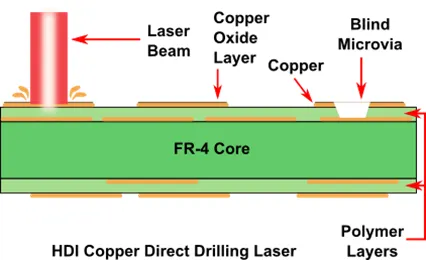
Laser Via vs Mechanical Via in HDI PCB: Which One Should You Use?
Blind and Buried Vias: The Hidden Heroes of HDI PCB Design
Blind Via Layout and Testing: Ensuring Quality and Reliability in PCB Manufacturing
Microvia Design for EMI Reduction
Microvia Stackup: The Complete Beginner's Guide
The Art of Microvia Placement
Stacked Via vs. Via in Pad: Which Via Technology is Best for BGA Routing?
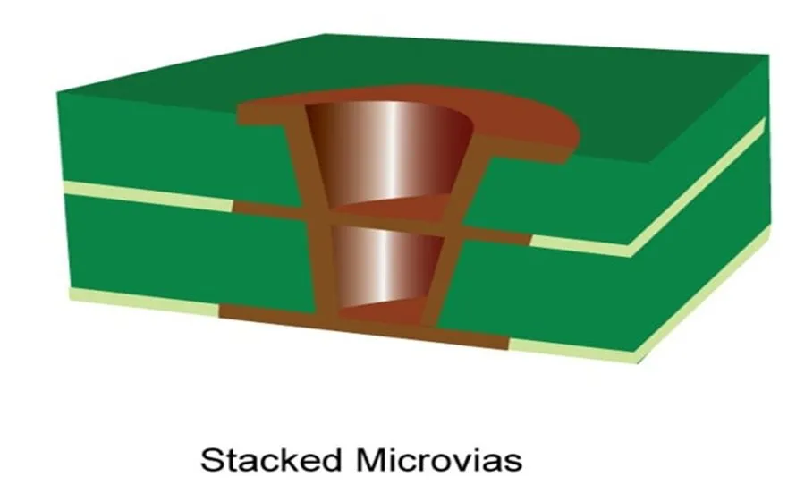
Stacked Microvias: Enabling High Density Interconnects for Advanced Electronics
Best Practices for Plating Stacked Vias: Achieving Uniform Copper Deposition
Blind Via Placement Strategies for Optimal Signal Integrity
What Are the Benefits of Blind Vias?
The Essential Role of Blind Vias in HDI PCBs
Microvia PCB Design Rules: A Practical Handbook for Error Free HDI Layouts
Get in Touch
Send Message
- Products & Service
- Company
- About AIVON
- Contact
- News
- Blog
- Certification
-


- Payment
-


2026 AIVON.COM All Rights Reserved