 00:57
00:57
Via Reliability
Via reliability is a critical aspect of printed circuit board (PCB) design and manufacturing, focusing on the durability and performance of vias that interconnect multiple layers in complex electronic assemblies. These conductive pathways, essential for signal routing and power distribution, can be prone to failures such as cracking, delamination, or voiding due to thermal cycling, mechanical stress, or manufacturing defects. For engineers, designers, and manufacturers searching for information on via reliability, this tag aggregates expert insights into the factors that influence via integrity, helping to mitigate risks in high-stakes applications like aerospace, automotive, and consumer electronics. Understanding via reliability involves evaluating key parameters such as aspect ratio, plating thickness, and material selection to ensure long-term stability under operational conditions. Practical applications include implementing design rules that optimize via placement and size, as well as adopting advanced techniques like filled vias or laser-drilled microvias for enhanced thermal management. Best practices emphasize rigorous testing methods, including thermal shock cycling and shear strength assessments, to predict and prevent failures before they impact product performance. By addressing these elements, professionals can achieve higher yield rates in production and reduce costly rework or field failures. The articles linked under this tag delve into real-world case studies, simulation tools, and industry standards that provide actionable strategies for improving via reliability. Whether you are troubleshooting existing designs or planning new ones, these resources offer valuable guidance to enhance PCB robustness and meet stringent reliability requirements.
Video Guide
-
00:57
Technical Articles
Via Design Guidelines in PCB Design: Balancing Performance and Cost

Why Traces Can Still Open After Teardrops Are Added to Vias
How We Fixed Solder Mask Bridges, Copper Density & Via Issues in Thin 6-Layer HDI PCB
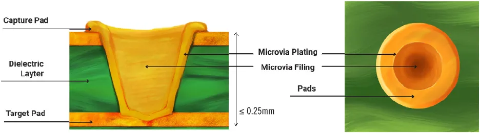
High Aspect Ratio PCBs: Challenges, Solutions, and Advanced Manufacturing Techniques
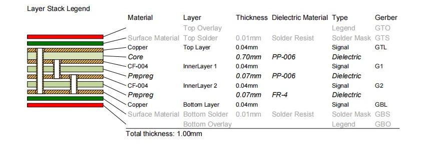
Advanced PCB Materials: Enhancing Blind and Buried Via Performance
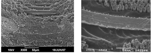
Advanced PCB Etch Back Techniques Using Plasma: Improving Interlayer Connections
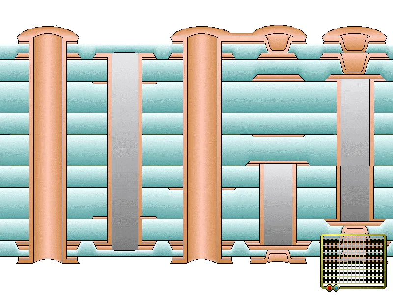
Stacked Via PCBs in Medical Devices: Ensuring Performance and Safety
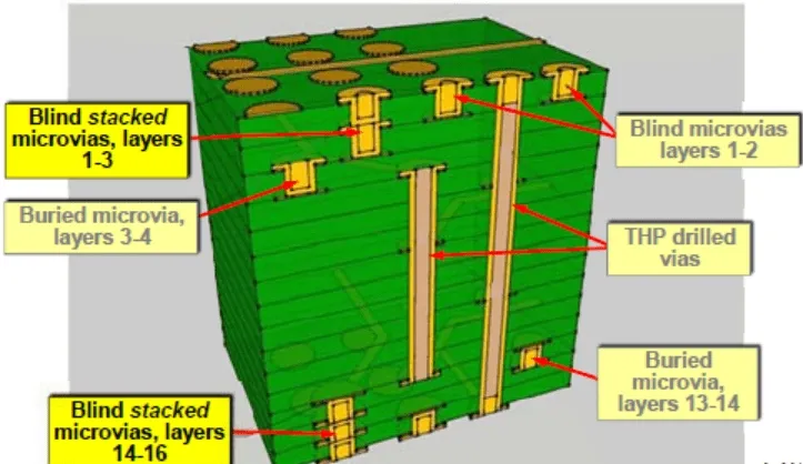
Troubleshooting Stacked Via Problems: A Practical Guide
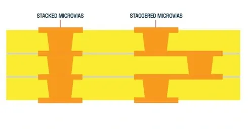
Stacked Vias vs. Staggered Vias: Choosing the Right Via for Your PCB Project
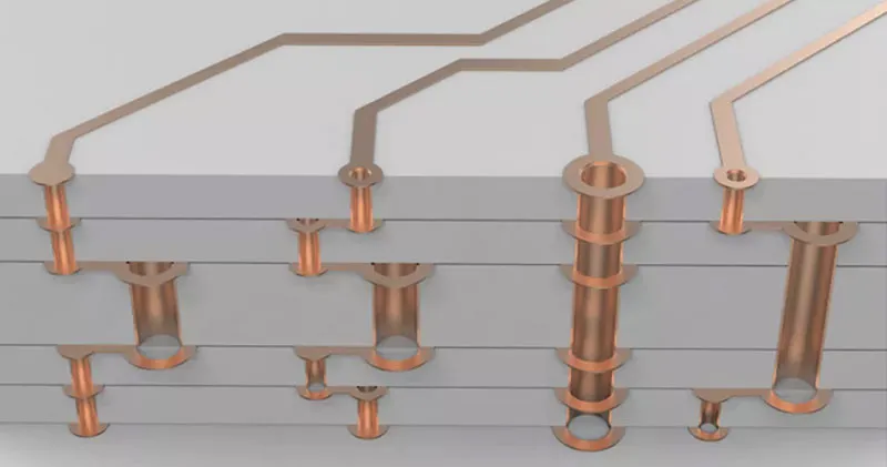
Through Hole Via Reliability: Common Failure Modes and Prevention
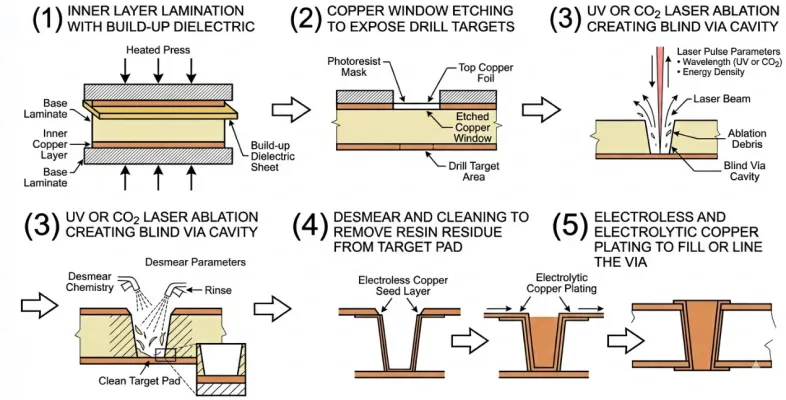
HDI Laser Drilling Mistakes That Affect Manufacturing Yield
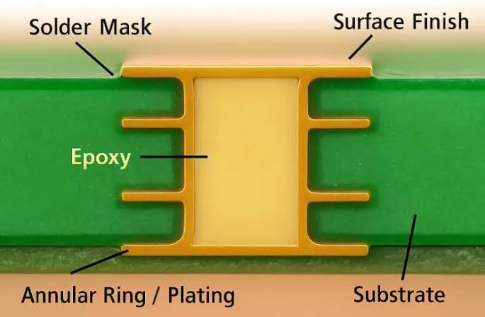
Resin Filled Via vs Copper Filled Via HDI: What Is the Difference?
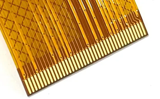
Should Via Openings Be Kept on FPC Boards?
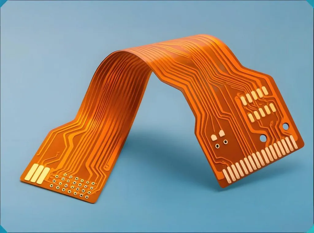
Canceling Via Openings on FPC to Prevent Long-term Oxidation
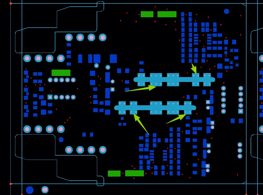
How DFM Review Prevented Via Reliability Risks in a 2-Layer FR4 PCB
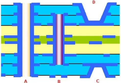
High Reliability Blind Via Design: Meeting Stringent Industry Standards
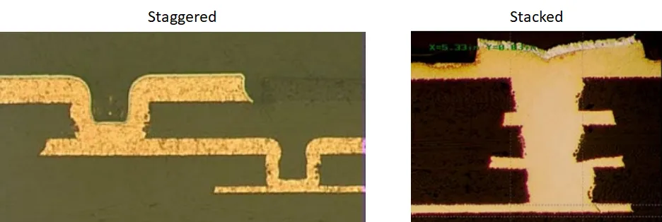
Troubleshooting Microvia PCB Defects: A Guide to Identifying and Resolving Common Issues
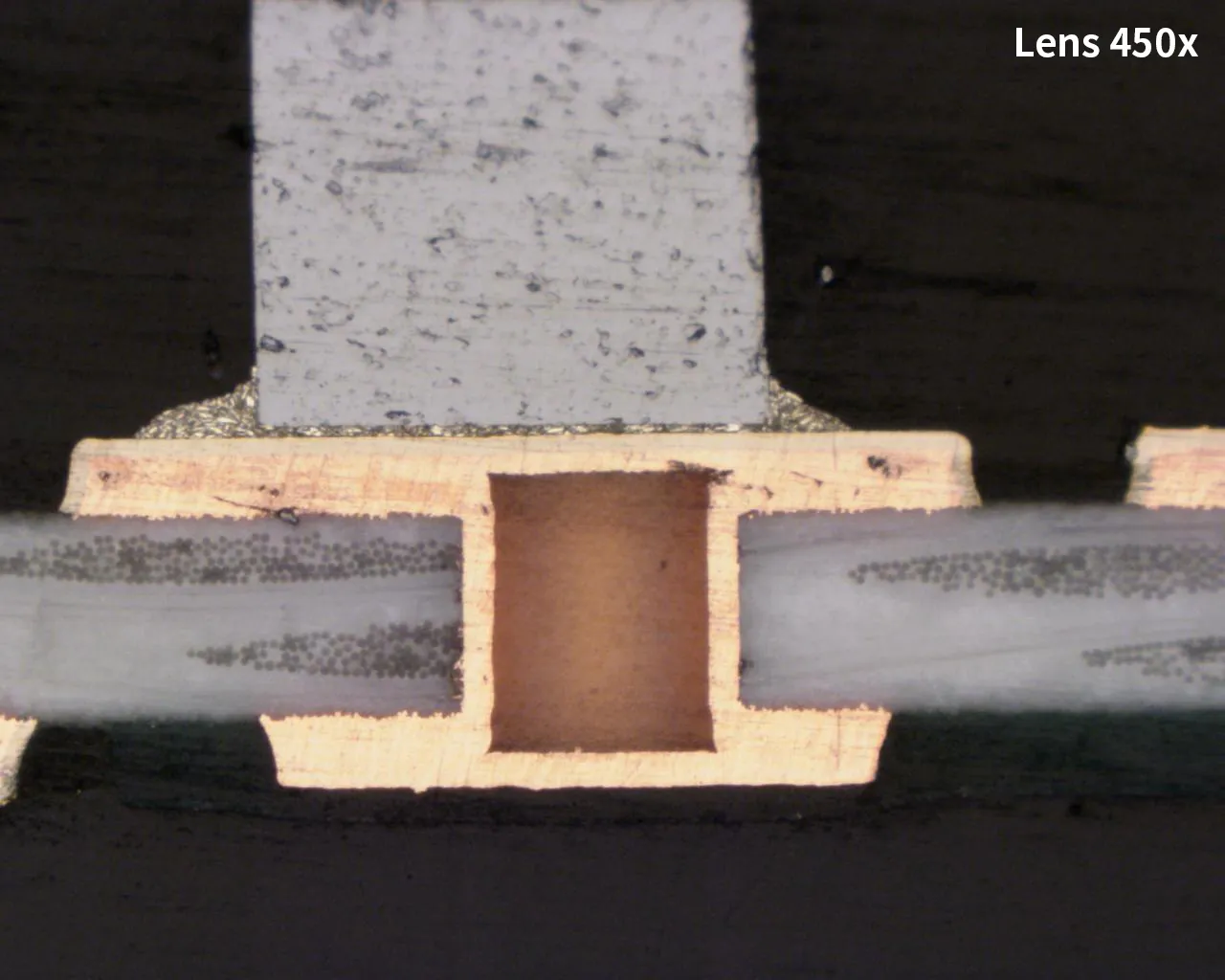
The Role of Via Filling in Via in Pad Reliability
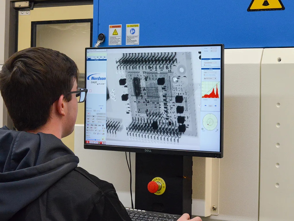
X Ray Vision for PCBs: Mastering Defect Detection in Electronics Manufacturing