Introduction
High aspect ratio PCBs play a critical role in modern electronics where dense interconnects and multilayer configurations demand reliable through-hole vias in thicker boards. These boards enable compact designs for applications like power supplies, automotive systems, and telecommunications equipment by allowing smaller diameter holes relative to board thickness. However, high aspect ratio PCB manufacturing introduces significant hurdles in drilling, plating, and reliability testing that can compromise performance if not addressed properly. Engineers must understand these challenges to select appropriate design rules and manufacturing partners. This article explores the definition, key issues such as PCB plating challenges and via cracking, practical solutions, and advanced techniques grounded in industry practices. By focusing on factory-driven insights, it provides actionable guidance for achieving robust high aspect ratio boards.
What Is a High Aspect Ratio PCB and Why Does It Matter?
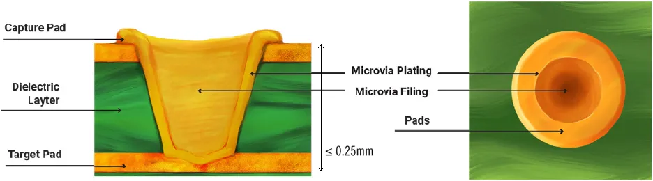
The aspect ratio of a PCB is defined as the ratio of the board's thickness to the diameter of the drilled via or hole. A high aspect ratio typically exceeds 10:1, meaning a board thicker than 10 times the hole diameter, such as a 2 mm thick board with 0.2 mm holes. Standard boards often operate at 6:1 to 8:1 ratios, but high aspect ratios become necessary for high-layer-count designs requiring fine-pitch vias to maximize routing density. This configuration supports more traces per layer and reduces overall board size, which is vital for space-constrained products. In high aspect ratio PCB manufacturing, exceeding common limits pushes the boundaries of process control, directly impacting yield and long-term reliability. Engineers prioritize this metric early in design to align with fabrication capabilities and avoid costly redesigns.
Key Challenges in High Aspect Ratio PCB Manufacturing
Drilling high aspect ratio vias presents mechanical difficulties due to increased depth, leading to issues like drill bit deflection, breakage, and poor chip evacuation. Thinner drills wander more in deep holes, compromising hole position accuracy and wall quality, which sets the stage for plating defects. Factories mitigate this through peck drilling cycles and optimized feed rates, but higher ratios amplify these risks. PCB plating challenges intensify with aspect ratios above 10:1, as electroplating solutions struggle to deposit uniform copper thickness along the via barrel. The plating throw power, or ability to coat deep recesses evenly, diminishes, resulting in thinner copper at the via bottom and potential voids or seams. These inconsistencies weaken the conductive path and increase resistance, critical for high-current applications.
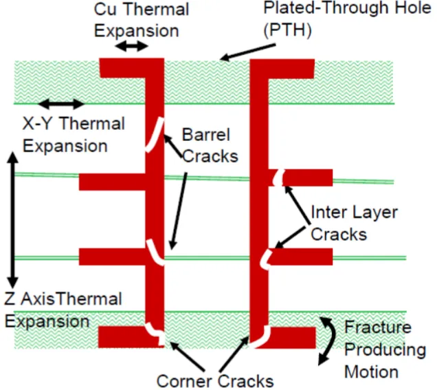
Via cracking emerges as a primary reliability concern in high aspect ratio boards, often manifesting as barrel cracks during thermal cycling or assembly reflow. The copper plating experiences shear stress from differential expansion between the metal and dielectric, exacerbated by the elongated via geometry. Micro-cracks propagate under repeated stress, leading to open circuits over time. Z-axis expansion further compounds this, as laminates like FR-4 exhibit significant thickness swelling above their glass transition temperature, potentially causing delamination or inner layer separation. IPC-2221 guidelines highlight how Z-axis expansion above Tg can be four times greater than in-plane, stressing via interfaces. Warpage also arises from plating stresses and asymmetric buildup, distorting flatness and complicating assembly.
Practical Solutions and Best Practices
Designers address high aspect ratio challenges by optimizing via diameters to maintain ratios below 12:1 where possible, balancing density with manufacturability. Staggering via locations across layers reduces cumulative stress concentrations, while using filled or blind vias in outer layers minimizes through-hole depth. Material selection plays a pivotal role; low-CTE resins and high-Tg laminates per IPC-4101 specifications limit Z-axis expansion, enhancing thermal stability. Balanced stackups with symmetric copper distribution counteract warpage tendencies during lamination and plating. Pre-treatments like plasma desmear improve surface activation for better plating adhesion, reducing void risks.
In manufacturing, factories employ multi-stage plating sequences to overcome PCB plating challenges. Direct metallization followed by pulse electroplating enhances throw power, delivering more uniform deposits in deep vias compared to traditional DC methods. Vertical plating racks with agitation systems ensure electrolyte renewal at via bottoms, critical for high aspect ratios. Post-plating anneals relieve internal stresses, minimizing via cracking propensity. IPC-6012E qualification tests verify plating integrity through cross-section analysis and thermal shock cycling. Routine inspections via automated optical systems detect early warpage or plating anomalies, allowing process adjustments.
Advanced Manufacturing Techniques for High Aspect Ratio PCBs
Advanced PCB equipment elevates high aspect ratio PCB manufacturing by incorporating precision drilling and plating innovations. High-pressure coolant systems in mechanical drills facilitate chip removal in ratios up to 15:1, paired with entry and backup materials to prevent burrs. Laser drilling complements for entrance quality, though reserved for blind vias due to taper in through-holes. Flip-drill techniques process boards from both sides sequentially, halving effective aspect ratios during plating and improving uniformity.
Electrochemical innovations like periodic reverse plating address throw power limitations, oscillating current direction to dissolve excess surface copper and redistribute into depths. This yields bottom-to-top thickness ratios closer to 1:1 even at 12:1 aspects. Controlled impedance plating maintains via resistance profiles for signal integrity. Post-process via filling with conductive epoxies reinforces barrels against cracking, enabling even higher densities. IPC-A-600K acceptability criteria guide these enhancements, ensuring class 3 reliability for demanding sectors.
Integration of in-line metrology, such as X-ray laminography, monitors Z-axis expansion and plating voids non-destructively. Factories calibrate advanced PCB equipment for specific resin systems, optimizing parameters like current density and bath chemistry. These techniques collectively boost yields from below 80% at extreme ratios to over 95%, as process windows widen.
Conclusion
High aspect ratio PCBs demand meticulous attention to design, materials, and processes to overcome inherent challenges like PCB plating challenges, via cracking, and Z-axis expansion. By adhering to aspect ratio limits, leveraging high-Tg materials, and deploying advanced manufacturing techniques, engineers achieve reliable boards for high-density applications. Factory insights emphasize proactive controls, from optimized drilling to pulse plating, aligned with IPC standards for qualification. Selecting partners proficient in advanced PCB equipment ensures consistent outcomes. Ultimately, balancing performance and manufacturability unlocks the full potential of these complex boards in evolving electronics landscapes.
FAQs
Q1: What are the main PCB plating challenges in high aspect ratio PCB manufacturing?
A1: PCB plating challenges arise from reduced throw power in deep vias, leading to uneven copper distribution with thinner deposits at the bottom. Factories counter this using pulse plating and enhanced agitation to improve electrolyte access. Adhering to aspect ratios under 12:1 further aids uniformity, preventing voids that compromise conductivity. Standards like IPC-6012E guide plating thickness verification through cross-sections.
Q2: How does via cracking occur in high aspect ratio boards, and what prevents it?
A2: Via cracking stems from thermal mismatch stresses elongating the copper barrel during cycling, common above 10:1 ratios. Z-axis expansion amplifies this by swelling the dielectric unevenly. Prevention involves high-Tg laminates, stress-relief annealing, and balanced designs per IPC-2221. Routine thermal shock testing identifies risks early.
Q3: What role does Z-axis expansion play in high aspect ratio PCB reliability?
A3: Z-axis expansion causes thickness swelling in laminates above Tg, stressing via walls and risking cracks or delamination. High aspect ratios intensify this due to longer stress paths. Solutions include IPC-4101-compliant low-expansion materials and symmetric stackups to maintain integrity under reflow.
Q4: Why is advanced PCB equipment essential for high aspect ratio vias?
A4: Advanced PCB equipment like high-pressure drills and vertical plating systems handles deep holes with precision, ensuring chip evacuation and uniform plating. It enables ratios up to 15:1 while minimizing defects. Such tools integrate metrology for real-time adjustments, boosting yields in demanding production.
References
IPC-2221 — Generic Standard on Printed Board Design. IPC, 2012
IPC-6012E — Qualification and Performance Specification for Rigid Printed Boards. IPC, 2017
IPC-A-600K — Acceptability of Printed Boards. IPC, 2020
IPC-4101 — Specification for Base Materials for Rigid and Multilayer Printed Boards. IPC, 2017


