










In multilayer PCB design, vias are the critical interconnect structures that link circuitry across layers. Their geometry and placement directly affect electrical performance, manufacturability, cost, and long-term reliability. Drilling alone can account for 30%–40% of PCB manufacturing cost, so striking a balanced design that supports high-speed, high-density routing without driving up cost is a key engineering challenge. This article consolidates practical design rules and shop-floor considerations to help you avoid common pitfalls in via design.
Via Dimensions: Smaller Is Not Always Better—Respect Process Limits
A via consists of a drilled hole and its surrounding pad. Size selection should follow both electrical needs and process capability:
- Baseline inner and outer diameters: For through-hole vias, an inner diameter of ≥0.2 mm (8 mil) and an outer diameter of ≥0.4 mm (16 mil) are recommended. In extreme cases the outer diameter may be reduced to 0.35 mm (14 mil), but this pushes process limits.
- Empirical sizing rule: The via pad diameter is typically around two times the drill diameter ±2 mil. For example, an 8 mil drill commonly uses a 14/16/18 mil pad depending on stack-up and fab capability.
- Process constraints: Reducing drill size increases the risk of drill wander and breakout. When the via aspect ratio (board thickness to finished hole diameter) exceeds roughly 6:1, it becomes difficult to maintain plating uniformity and via reliability.
- Design guidance: For high-speed nets, smaller vias help reduce parasitic capacitance, but do not chase minimums blindly. Confirm the fabricator's proven capability and stay within robust process windows.
Blind and Buried Vias: Use Low-Order Microvias Judiciously
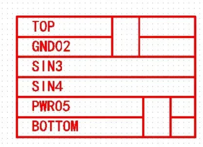
For BGA packages with pitch ≥0.65 mm, avoid blind and buried vias whenever possible due to cost and process complexity. If blind vias are required, use first-order microvias (for example, TOP–L2 or BOTTOM–L2) with an inner diameter around 0.1 mm (4 mil) and an outer diameter around 0.25 mm (10 mil). Higher-order microvias do increase routing density, but fabrication difficulty and cost escalate rapidly, often outweighing the benefit for mainstream designs.
Vias and Pads: Avoid Tombstoning and Solder Wicking
Placing a via directly in a component pad can reduce interconnect inductance, but it also allows solder paste to wick into the via barrel during reflow. This depletes solder volume and can cause tombstoning or opens. Use via-in-pad only when absolutely required and with proper via filling and capping processes.
- Clearance to pads: Maintain 4–8 mil clearance between a via edge and a solder pad edge to avoid solder bridging and to improve assembly yield.
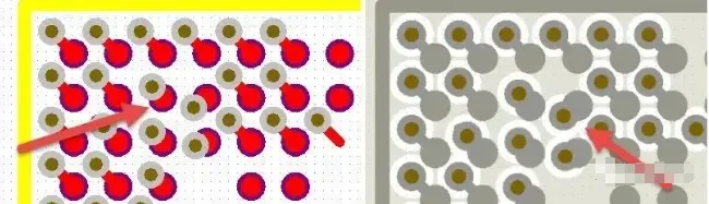
- In BGA regions: Place escape vias on the centerline between adjacent pads, not inside BGA pads. After drilling, use via filling and solder mask over (plug and cap) processes so the BGA solder balls sit flat and solder volume remains consistent.
Via-to-Via Spacing: Prevent Breakout and Protect Reliability
Overly tight via spacing increases the risk of breakout and drill damage. Observe robust spacing rules:
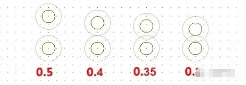
- Minimum spacing: A center-to-center via spacing of ≥0.5 mm is recommended. Avoid 0.35–0.4 mm if possible, and do not use ≤0.3 mm due to high risk of defects.
- High-density areas: Use staggered arrangements and tune via diameters to improve utilization while maintaining mechanical integrity.
Via Filling and Solder Mask Over: Critical for Soldering Yield
For small-diameter vias (≤0.5 mm) and specific assembly scenarios, via filling and solder mask capping are required:
- Under metal-can or metal-cased components: Fill and cap vias under the component body to prevent accidental shorting to the case.
- Thermal via exception: For heat-spreading vias, open vias may be retained to enhance heat transfer, provided assembly considerations are addressed.
Reinforcing Mechanical Pads with Vias
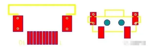
Pads that experience mechanical stress—such as audio jacks, buttons, or FPC connectors—are prone to pad lifting if not reinforced. Add one or two evenly spaced stitching vias tied to the pad or its copper pour to increase copper adhesion and improve mechanical robustness.
Fanout Design: A Win–Win for Signal Integrity and Cost
1. Fanout for Common Chip Components
Place escape vias on the outer side of chip components so inner-layer routes can pass between adjacent vias without slotting or cutting the reference plane. This preserves plane continuity and reduces impedance discontinuities. Incorrect fanout placement increases routing difficulty and can disrupt power or ground planes.
2. BGA Fanout
Align escape vias precisely within their own via pads, and do not offset them into BGA solder pads. Avoid via-in-pad unless the process explicitly includes via filling and capping; unfilled via-in-pad can cause solder voids and opens. Poor BGA fanout can also slot or fragment power/ground planes, creating impedance discontinuities and degrading signal integrity.
Conclusion: Apply Rules Rigorously and Sweat the Details
Via design is a leverage point in PCB engineering: small decisions can drive large outcomes in performance, cost, manufacturability, and reliability. By choosing sensible via sizes, enforcing robust spacing, and applying disciplined fanout strategies, you can meet high-speed design needs while controlling cost. Equally important is early and close communication with your PCB fabricator to align on proven process capabilities, so that well-conceived design rules translate into consistently buildable, reliable hardware.






