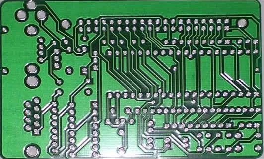
Exposed vias on flex circuits create real headaches down the line. The combination of FPC via opening oxidation and flex PCB via exposure risk shows up often enough in DFM reviews that it's worth a close look before you finalize your layout.

Why Exposed Vias Become a Problem Over Time
On rigid boards we sometimes leave vias open without much concern. FPCs are different. The thin, flexible base and the way coverlay is applied change the exposure dynamics completely.
Copper that stays uncovered oxidizes. In normal office or consumer environments this might take months or years. Put the board into automotive, industrial, or high-humidity conditions and the timeline collapses.
Oxidation Process in Practice
Exposed copper first forms a thin oxide layer. That layer isn't always a disaster for electrical contact if you're probing immediately after fabrication. But over time it thickens, especially with sulfur or chlorine in the air. Contact resistance climbs. In high-current paths or signal vias this matters.
Worse, the oxide can migrate under the coverlay edge. You end up with delamination starting right at the via rim. I've seen boards come back after six months in the field with intermittent opens that trace straight to this mechanism.

Flex PCB Via Exposure Risk During Assembly and Use
Assembly adds another layer. Flux residues love to hide in open vias. Cleaning flex circuits thoroughly is harder than rigid ones. Residual flux plus exposed copper equals accelerated corrosion.
Dynamic bending makes things uglier. Every flex cycle stresses the coverlay-to-copper interface around the via. Micro-cracks form. Moisture gets in. The FPC via opening oxidation accelerates and reliability drops fast.
Thermal cycling compounds the issue. Different CTEs between copper, polyimide, and coverlay create shear forces right at the exposed edges.
Common Failure Modes Engineers See
- Increased contact resistance on test points or connectors
- Intermittent signal integrity problems after humidity exposure
- Delamination starting at via openings during repeated flexing
- Solder wicking into vias during reflow if openings are too generous
Factory Perspective on Canceling Via Openings
Most FPC manufacturers prefer to cover vias completely with coverlay when possible. The process is straightforward. They register the coverlay film, punch or laser the openings only where you actually need pads exposed, and leave everything else protected.
From the CAM side, keeping openings means tighter registration requirements. Any misalignment and you get partial coverlay on pads or excessive exposure around vias. Covering them removes that variable.

Electrically it makes little difference in most designs. The via is still there for layer connection. The coverlay doesn't block the hole — it just protects the annular ring and top copper.
When Keeping Openings Might Still Make Sense
Not every via should be covered. Test points that need frequent probing during development or in-field diagnostics are obvious candidates. Some connector footprints benefit from exposed areas for better solder fillet inspection.
High-density designs sometimes force trade-offs. If coverlay registration windows can't guarantee clean pad exposure without risking via openings, you have decisions to make.
Practical Layout Rules to Reduce Exposure Risk
Start by flagging which vias truly need to stay open. Everything else gets covered.
Keep annular rings generous when you do expose vias — at least 0.15 mm on each side for most processes. This gives the coverlay a better landing area if slight misalignment occurs.
Consider filled vias for critical areas. Not every fab offers this on flex at reasonable cost, but when available it eliminates the exposure issue entirely.
For dynamic flex zones, avoid placing vias in the bend area altogether when possible. If you must, cover them and use staggered or elongated pads to distribute stress.
Making the Call on Your Specific Design
Look at the environment first. Consumer gadgets in dry conditions might tolerate a few exposed vias. Medical, automotive, or outdoor IoT devices usually cannot.
Check your reliability requirements. If the product needs to pass 85/85 humidity testing or extended temperature cycling, covering vias becomes almost mandatory.
Talk to your fab early. Their coverlay process capabilities and typical registration tolerances will tell you what's realistic. Some can hold ±0.05 mm. Others need more margin.
Design Checklist Before Tape-Out
- Identify every via that can be covered without affecting function
- Verify coverlay opening sizes match your pad requirements with margin
- Confirm via placement avoids high-flex zones when exposed
- Specify ENIG or other protective plating if any exposure remains
- Document which vias are intentionally left open and why
The extra communication step with the manufacturer pays for itself in fewer surprises during first article inspection.
In most modern FPC designs, the safest default is to cover vias unless there's a clear reason not to. The flex PCB via exposure risk is real, and preventing FPC via opening oxidation is usually cheaper than chasing field failures later.
Review your next layout with this in mind. Small changes in coverlay strategy can make a noticeable difference in long-term reliability.