Copper separation in plated-through holes is not caused by a single electroplating parameter. The adhesion and reliability of barrel copper are established progressively through the substrate, drilling, desmear, hole-wall treatment, activation, electroless copper deposition, and electroplating processes. If a weak interface forms at any stage, later processing may not be able to compensate for it.
What Factors Affect Plated-Through-Hole Copper Adhesion?
1. Base Material
The resin system, glass-fabric structure, resin content, and quality of the glass-fiber-to-resin interface all affect plated-through-hole reliability.
The difference in thermal expansion between glass fibers and resin influences the mechanical stress applied to barrel copper during thermal cycling. When different materials are laminated together, their thermal expansion characteristics may not match. This mismatch increases the reliability risk for plated-through holes because the copper barrel must accommodate the resulting thermomechanical stress.
2. Drilling Quality
Drill wear, spindle speed, feed rate, chip evacuation, and drilling temperature all affect the condition of the hole wall.
Excessive drilling heat can produce resin smear. Tears, burrs, protruding glass fibers, and abnormal roughness on the hole wall can also interfere with the bonding of subsequent copper layers. These defects may prevent the surface from being properly cleaned, activated, and covered by a continuous electroless copper layer.

3. Desmear and Hole-Wall Treatment
Insufficient desmear leaves resin residue on the hole wall, preventing the subsequent activation and electroless copper processes from making adequate contact with the substrate.
Over-processing creates a different problem. Excessive resin erosion, recessed glass fibers, or an abnormal hole-wall profile can reduce reliability even when the hole appears clean. The objective is therefore not to make desmear as aggressive as possible, but to maintain an appropriate and uniform process window.

4. Hole-Wall Surface Condition
Appropriate surface roughening helps increase the mechanical interlocking between the copper layer and the resin. However, excessive roughening, severe glass-fiber recession, or an uneven interface can create localized stress concentrations. A surface that is too rough or irregular may therefore be just as problematic as a surface that has not been adequately prepared.
5. Cleaning, Activation, and Electroless Copper
Insufficient cleaning, contamination on the hole wall, or uneven activation can result in incomplete nucleation of the electroless copper layer.
Electroless copper provides the initial conductive and bonding layer for subsequent electrolytic copper plating. If the electroless copper contains areas of incomplete coverage, voids, or poor adhesion, increasing the thickness of the later electroplated copper cannot fully repair the original interface defect. The quality of the initial copper coverage is therefore critical to the reliability of the complete plated-through-hole structure.
6. Electroplating Conditions
Current density, solution movement, additive condition, plating time, and current distribution inside the hole all influence barrel copper quality.
High-aspect-ratio holes are particularly sensitive to plating distribution. The copper layer may become thicker near the hole entrances while remaining thinner in the center or at the bottom of the hole. This nonuniformity can reduce the available reliability margin and make the barrel more vulnerable to thermomechanical stress.
7. Thermomechanical Stress
Reflow, thermal shock, and repeated thermal cycling generate stress because copper and resin have different coefficients of thermal expansion.
If the hole wall already contains microcracks, interface defects, or areas of insufficient adhesion, thermal cycling can cause these defects to grow into hole-wall separation or barrel copper cracks. A board that passes a basic electrical continuity check may still contain a latent reliability problem that becomes visible only after thermal stress.
Special Designs That Can Reduce Copper Adhesion or Reliability
1. High-Aspect-Ratio Holes
As board thickness increases and hole diameter decreases, chemical exchange inside the hole becomes more difficult. Desmear uniformity and copper-plating distribution also become harder to control. The combination of a thick board and a small hole should therefore receive particular attention during design and fabrication planning.
2. Very Small Holes in Thick Boards
Small holes in thick boards do not only increase drilling difficulty. More importantly, they reduce the uniformity of chemical treatment and electroplating inside the hole. Design review should not stop at verifying whether the hole can be drilled. The fabricator's actual capability for cleaning, activating, and plating the hole should also be confirmed.
3. Large Variations in Hole Diameter on the Same Board
When small vias, large holes, and conventional through-holes are present on the same board, the chemical exchange and current distribution are different for each hole size. Maintaining all hole types within their optimum process conditions becomes more difficult, which can increase the risk of nonuniform copper coverage and reliability variation.
4. Laser-Microvia Structures
Resin residue, carbonized material, or insufficient cleaning at the bottom of a laser-drilled microvia directly affects the bond between the deposited copper and either the base material or the underlying copper layer.
Microvia depth, diameter, and bottom structure must be compatible with the actual laser-drilling and copper-plating capabilities available for the design. A microvia should not be evaluated only by its nominal geometry; the condition of the via bottom and the ability to achieve reliable subsequent copper coverage are equally important.
5. Special Structures Near Inner-Layer Copper
Resin smear remaining on an inner-layer copper surface can create a weak interface between the plated-through-hole copper and the inner-layer copper. On the other hand, excessive desmear can produce excessive resin recession or expose glass fibers, which can also reduce reliability.

6. Thick and Multilayer Boards
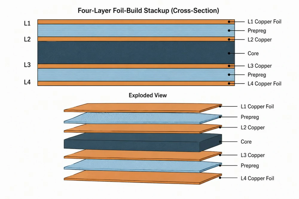
As board thickness increases, the thermomechanical stress applied to the barrel copper generally becomes more significant. A higher layer count does not automatically reduce copper adhesion, but it makes the material combination, drilling, desmear, and plating processes more complex to control.
7. Mixed-Material Laminations
When different resin systems, glass-fabric structures, or materials with different thermal expansion characteristics are combined in one stackup, thermal cycling can produce more complicated interface stress. These structures require process conditions that are suitable for the complete material system rather than for only one material used in the stackup.
8. Rigid-Flex Boards and Special Adhesive Layers
Polyimide, adhesive layers, and other flexible-circuit materials have chemical and processing characteristics that differ from those of conventional epoxy-based rigid-board materials. Standard rigid-board desmear and surface-treatment conditions should therefore not be applied without confirming their suitability for the special structure.
Key Design Considerations
The reliability chain can be summarized as:
Board thickness and hole diameter → hole aspect ratio → material and thermal-expansion characteristics → drilling quality → desmear level → hole-wall surface condition → activation and electroless copper coverage → electroplating uniformity → thermal-cycle reliability.
The most important design considerations are the following:
- Do not evaluate only the minimum hole diameter. Consider board thickness and hole aspect ratio at the same time.
- Do not specify only that the hole must be completely free of resin smear. The uniformity and degree of desmear must also be controlled.
- Do not evaluate only the final barrel copper thickness. Confirm the initial adhesion and coverage quality of the electroless copper layer.
- Treat thick boards, small holes, high-aspect-ratio holes, and mixed-material laminations as high-risk combinations.
- For laser microvias, verify hole-bottom cleanliness, the condition of the underlying copper, and the capability of the subsequent copper-plating process.
- For special structures, confirm the fabricator's process capability during the design stage rather than attempting to compensate after mass production by simply increasing copper thickness.
- Do not judge the result only by electrical continuity. Cross-sectional analysis, hole-wall inspection, and thermal-reliability testing should also be used for final evaluation.
Barrel copper adhesion is not determined by a single electroplating parameter. It is built progressively through the substrate, drilling, desmear, activation, electroless copper, and electrolytic copper stages. Once a weak interface has formed, subsequent processing may not be able to restore the lost reliability margin.
Use the Separation Location to Guide Failure Analysis
A. Separation Between the Barrel Copper and the Resin
Separation at the barrel-copper-to-resin interface generally points toward a hole-wall adhesion or pretreatment issue. In this case, the size and condition of the inner-layer land may have a limited influence compared with the quality of the hole-wall preparation.
B. Separation Between the Barrel Copper and the Inner-Layer Copper Land
When separation occurs at the connection between barrel copper and the inner-layer copper land, the land geometry and interface quality become especially important. The analysis should consider the inner-layer land size, land integrity, inner-layer copper thickness, and the quality of the copper-to-copper interface.
C. Separation Between the Inner-Layer Copper Land and the Surrounding Resin
This failure location requires consideration of post-separation around the inner-layer land after exposure to thermomechanical stress. The land may initially appear connected, but thermal cycling can cause separation at the interface between the inner-layer copper and the surrounding resin.
In plated-through-hole defect classifications, hole-wall pullaway and inner-layer post-separation are treated as different defect types. Identifying the exact separation location is therefore essential because it determines which process stage and structural feature should receive priority during failure analysis.