From the PCB manufacturing perspective, why can a trace designed for 50 Ω measure 53 Ω on the finished board? This is a common issue in PCB production. The first questions are often: Was the trace width incorrect? Was the copper over-etched? Was the material Dk different from the value used in the design? Any of these explanations may be possible, because PCB impedance is never determined by a single factor.
For a manufacturer, impedance is the combined result of trace geometry, layer structure, material properties, and process tolerances. The front-end engineer defines an ideal structure, while the PCB manufacturer must control the actual structure of the finished board. Any deviation between the two can change the measured impedance.
Why Can a Small Trace-Width Difference Change the Impedance?
Assume that a high-speed signal trace has a target impedance of 50 Ω and a designed width of 4 mil. It is tempting to assume that producing a 4 mil trace will automatically result in a 50 Ω impedance. In practice, the situation is more complicated because PCB traces must pass through exposure, development, etching, and other manufacturing processes.
The 4 mil value in the design represents a theoretical dimension. The final trace width on the manufactured PCB is affected by etch compensation, etch rate, copper thickness, trace density, and other process conditions. During etching, copper is removed not only in the vertical direction but also laterally. This lateral etching is commonly referred to as undercutting.
As a result, the cross-section of a finished trace is usually not an ideal rectangle. It may have a trapezoidal profile. The designed trace width therefore does not necessarily equal the final trace width. Once the trace width changes, the impedance changes as well. With all other conditions held constant, a narrower trace generally produces higher impedance, while a wider trace generally produces lower impedance.
PCB manufacturers use etch compensation so that the final trace width falls as close as possible to the target range. This is why it is not sufficient to say that the Gerber file specifies 4 mil and the PCB factory produced 4 mil. The dimension that must ultimately be controlled is the trace width on the finished board.
Why Can the Impedance Be Incorrect When the Trace Width Is Correct?
The next major factor is dielectric thickness. If a signal trace is routed above a continuous reference plane, the distance between the trace and the reference plane is a critical parameter in the impedance structure.
In general, the closer the trace is to the reference plane, the stronger the electromagnetic coupling between them and the lower the impedance tends to be. When the trace is farther from the reference plane, the impedance tends to increase.
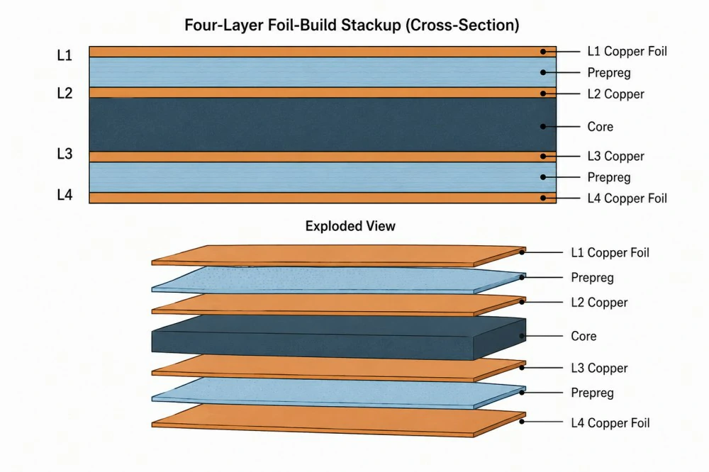
However, this distance is not determined entirely by the design engineer. It is also affected by the PCB lamination process. In multilayer boards, dielectric layers are commonly formed from prepreg and core materials. Before lamination, prepreg has a specified thickness and resin content. During lamination, its final thickness is affected by temperature, pressure, resin flow, and copper distribution.
Therefore, the nominal prepreg specification does not necessarily equal the final dielectric thickness after lamination. If the dielectric thickness changes, the impedance can shift accordingly. Some impedance problems that appear to be trace-related are actually caused by variations in the lamination structure.

Why Can Impedance Vary Between Batches of the Same Material?
This brings us to Dk, or dielectric constant. Dk is a critical parameter in impedance calculations, but it should not be treated as an absolutely fixed number by the manufacturing team.
PCB dielectric materials are composite structures made from glass fiber and resin. Their actual electrical properties can be affected by resin content, glass-weave structure, material formulation, frequency, degree of cure, and measurement method. In addition, the local ratio of glass fiber to resin is not necessarily uniform across the board. This creates an important high-speed PCB design issue known as the glass-weave effect.
When a high-speed trace passes through regions with different glass-fiber and resin distributions, the local dielectric environment seen by the signal can vary. At lower signal speeds, this effect may be less noticeable. As signal speed increases, however, it can affect impedance, propagation delay, and skew.
For this reason, high-speed PCB design should not ask only for the Dk value of a material. It is also necessary to understand the frequency, test method, and material structure associated with that Dk value. A Dk value obtained under one test condition may not accurately represent the effective dielectric behavior of a different PCB structure.
Why Can Two Boards Using the Same 1 oz Copper Have Different Impedance?
The term 1 oz primarily describes copper thickness. It does not fully describe the conductor. High-speed PCB design must also consider copper surface roughness.
As signal frequency increases, the skin effect becomes more pronounced and current becomes increasingly concentrated near the conductor surface. If the copper surface is relatively rough, the actual propagation path is affected more significantly. High-speed and high-frequency PCBs therefore often use low-profile or very-low-profile copper.
This is why copper selection for a high-speed PCB should not consider only whether the copper is 0.5 oz, 1 oz, or 2 oz. The surface characteristics of the copper are also important. In simplified terms, copper thickness may be the primary concern for lower-speed PCBs, while high-speed PCBs require attention to both copper thickness and copper surface profile.
Why Is 100 Ω Differential Impedance Not Simply Two 50 Ω Traces?
This is a common misunderstanding. Differential impedance is not obtained simply by adding the individual impedances of two traces. The two signal traces are electromagnetically coupled, so their differential impedance depends on the complete pair geometry.
Relevant parameters include trace width, trace spacing, copper thickness, dielectric thickness, and material Dk. Trace spacing is particularly important. As the two traces move closer together, coupling becomes stronger. As the spacing increases, coupling becomes weaker.
Therefore, a 100 Ω differential structure is a complete transmission-line design. It cannot be understood simply as 50 Ω + 50 Ω = 100 Ω. During PCB manufacturing, both trace width and trace spacing must be controlled for a high-speed differential pair. A trace-width result that meets its target does not guarantee that the differential impedance will also be correct if the spacing or dielectric structure has changed.

An Easily Overlooked Factor: Solder Mask
When engineers discuss PCB impedance, they often focus only on the copper trace and the dielectric layer below it. For an outer-layer microstrip, however, the solder mask above the trace is also a dielectric material.
The electrical environment around a trace is therefore different when solder mask is present and when it is absent. For a general-purpose PCB, this effect may not be the dominant factor. For high-speed, high-frequency, or tightly controlled impedance designs, however, the solder mask should be included in the analysis.
Relevant variables include solder-mask thickness, material properties, and the way the solder-mask opening is defined. An impedance model must consider not only what is below the copper trace, but also what is above it.
A Common Manufacturing Issue: Copper Distribution
Why do PCB manufacturers emphasize uniform copper distribution? The reason is not limited to preventing board bow and twist. Copper distribution also affects resin flow during lamination.
For example, one region of a panel may contain a high density of copper while another region contains very little copper. During lamination, resin flow and final dielectric thickness can differ between these regions. Because a change in dielectric thickness can also change impedance, copper balance has a direct relationship with impedance consistency in high-speed PCBs.
Uniform copper distribution is therefore relevant not only to mechanical stability but also to the consistency of the finished impedance structure across the panel and from one board region to another.
Why Can the Same Gerber Files Produce Different Results at Different PCB Factories?
This is one of the most important concepts in PCB impedance control. Gerber files primarily describe the design geometry of the PCB. They do not completely describe every physical property of the board after manufacturing.
Different PCB manufacturers may use different materials, prepreg combinations, copper foils, lamination conditions, etch compensation values, plating conditions, solder-mask processes, and process tolerances. As a result, even identical Gerber files can produce different physical structures at different factories.
Impedance is determined by the physical structure of the finished board. Consequently, the same digital design data does not guarantee the same impedance result unless the material system, stack-up, manufacturing process, and process controls are also sufficiently consistent.
Impedance Control Means More Than Producing One 50 Ω Trace
This is perhaps the most important point in PCB impedance control. The manufacturer's real challenge is not simply whether one trace can be produced at 50 Ω once. The more important question is whether an entire production batch can consistently meet the specified 50 Ω requirement.
These are fundamentally different objectives. The first is a one-time result. The second depends on overall process capability, beginning with incoming materials and continuing through lamination, circuit formation, plating, surface finishing, and final impedance testing.
PCB impedance is not determined by trace width alone. It is the combined result of trace width, copper thickness, dielectric thickness, Dk, trace spacing, conductor profile, material properties, lamination structure, and process tolerances.
When an impedance problem occurs, the investigation should therefore cover the complete manufacturing structure rather than focusing on trace width immediately. The relevant questions include:
- Has the trace width shifted from the target?
- Has the copper thickness changed?
- Does the dielectric thickness match the stack-up?
- Does the material Dk match the value used in the impedance model?
- Has etch undercut changed the conductor profile?
- Has lamination changed the dielectric thickness?
- Were solder mask and surface finish included in the impedance model?
- Are the impedance measurement method and process capability appropriate?
This is the correct way to understand PCB impedance from the manufacturing perspective. Although impedance control appears to be an electrical issue, it is actually a system-level engineering task spanning design, materials, and manufacturing.