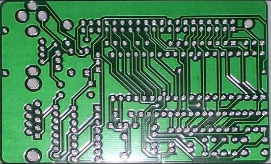
A PCB trace may occasionally include a localized solder mask opening even though the trace itself is not intended to be a test point, soldering pad, or connector contact. The purpose is usually to adjust the trace's surrounding dielectric environment and fine-tune its electrical characteristics.
The Main Purpose of a Local Solder Mask Opening
A solder mask opening changes the material above the copper trace from solder mask to air. Because these materials have different dielectric properties, the electric-field distribution around the trace also changes. As a result, the trace impedance may be adjusted over the exposed section.
- Without solder mask: The region above the trace is primarily air, which generally produces a lower effective dielectric constant and tends to increase the characteristic impedance, Z0.
- With solder mask: Solder mask typically has a higher dielectric constant than air. The electric field is more strongly loaded by the dielectric material, so the characteristic impedance generally decreases.
This makes it possible to use the opening's width, length, and position as local impedance-adjustment parameters. However, the opening is not electrically invisible. The transition between solder-mask-covered and solder-mask-free sections creates a change in the transmission-line environment and therefore forms an impedance discontinuity.
The practical objective is not simply to expose as much copper as possible. The actual objective is to achieve the required impedance while maintaining adequate impedance continuity, signal quality, and manufacturing reliability.
Key Design Considerations
1. Target Impedance
The target may be 50 Ω single-ended impedance or 90 Ω or 100 Ω differential impedance, depending on the interface and design requirements. If the selected trace width and PCB stackup produce an impedance that is slightly lower than the intended value, a localized solder mask opening may be used to increase Z0 in that region.
This adjustment should be based on an impedance model rather than on visual judgment. The model should include the actual stackup, copper geometry, reference-plane spacing, trace width, solder mask thickness, and solder mask dielectric properties whenever those parameters materially affect the result.
2. Impedance Continuity
The solder-mask-covered section and the opened section do not have the same dielectric environment. A high-speed signal therefore encounters a transition in the effective transmission-line geometry as it enters and leaves the opening.
If the impedance changes abruptly, part of the traveling wave can be reflected toward the driver. The resulting reflection may produce waveform distortion, overshoot, undershoot, or reduced timing and voltage margin. For this reason, a high-speed trace should not be designed with arbitrary alternating sections of solder mask and exposed copper.
A local opening should have a clear electrical purpose and should be evaluated as part of the complete signal path. The transition geometry at both ends is relevant, not only the central exposed region.
3. Opening Length
A short localized opening often has a relatively limited effect and can be used as a fine adjustment. However, increasing the opening length increases the distance over which the signal experiences the altered dielectric environment.
When the opening becomes sufficiently long relative to the signal's electrical length, it should be treated as a separate transmission-line section rather than as a negligible local feature. Its impedance, transitions, and interaction with the rest of the routing should then be included in the analysis.
4. Opening Width
The opening width affects more than the visible amount of exposed copper. It changes how much of the trace's electric field is surrounded by solder mask and how much is surrounded by air.
An opening that is too narrow may have only a limited effect on the effective dielectric constant and impedance. An excessively wide opening may create a larger transition in the field distribution and may increase the severity of the impedance discontinuity. The opening should therefore be sized according to the intended electrical correction rather than simply enlarged to maximize exposure.
5. Differential-Pair Symmetry
For a differential pair, the solder mask openings on the two traces should be highly symmetrical. The opening width, length, position, and transition geometry should match as closely as the manufacturing process permits.
Asymmetry can disturb the balance between the two conductors. It may change the differential impedance, create common-mode conversion, or introduce a relative delay between the pair members. These effects can degrade differential signal quality even when the average geometry appears acceptable.
6. Manufacturing Tolerances
The final electrical result depends on more than the nominal CAD geometry. Solder mask thickness, dielectric constant, opening dimensions, registration accuracy, and process variation can all affect the actual impedance.
Consequently, an idealized model that treats the area as either pure air or pure solder mask may not accurately represent production hardware. The impedance analysis should use realistic manufacturing assumptions, particularly when the opening is being used to correct a small impedance error rather than to create a large geometric change.
Does Opening Size Affect Product Performance?
Yes, but the degree of impact depends on the function of the region and the electrical speed of the signal.
High-Speed and Impedance-Controlled Traces
As the opening becomes larger, a greater proportion of the field around the trace is exposed to air instead of solder mask. The effective dielectric constant generally decreases, and the trace impedance generally increases.
An opening that is excessively wide or long may create a more significant impedance discontinuity. The resulting reflection can degrade the waveform and reduce the available sampling margin. The impact is determined by the complete geometry, including the reference plane, trace dimensions, dielectric thickness, and transition shape.
For differential pairs, unequal openings can cause differential-impedance imbalance and timing skew. Maintaining symmetry is therefore essential. The two traces should be treated as a coupled structure rather than as two independent single-ended traces.
Lower-Speed Control Traces
For an ordinary low-speed control trace, the electrical effect of a localized solder mask opening is often small compared with the effect on a high-speed interconnect. In such cases, the more important concerns may be surface protection, contamination, oxidation, appearance, and mechanical durability.
This does not mean that an arbitrary exposed section is automatically acceptable. The opening still needs to match the intended product function and manufacturing process.
Should the Opening Leave Bare Copper Exposed?
A solder mask opening does not necessarily mean that the copper will receive the same surface finish as the surrounding PCB. If the opened area has no ENIG, OSP, HASL, or other surface treatment, the copper is directly exposed to the environment. At that point, the primary concerns shift from impedance adjustment to copper-surface reliability and manufacturability.
- Oxidation: Bare copper can oxidize when exposed to air and moisture. Surface discoloration and degraded contact performance may result.
- Corrosion: High humidity, elevated temperature, and ionic contamination can increase the risk of corrosion.
- Contact reliability: If the area is contacted by a probe, spring contact, or connector, the copper surface condition directly affects contact resistance and service life.
- Solderability: If the location may need to be soldered later, copper oxidation can create solderability problems.
- Mechanical wear: Bare copper has no solder mask protection and may be damaged by friction or repeated contact.
- Insulation reliability: Ionic contamination and conductive-anodic-filament-related risks require particular evaluation in high-humidity or high-voltage environments.
Therefore, exposed copper should not be regarded as an automatic substitute for a solder mask opening. If the exposed copper is intentionally designed as part of the PCB process and the region is explicitly specified to remain untreated, it cannot be judged acceptable or unacceptable without considering its function and operating environment.
When Can Exposed Copper Be Intentional?
Different applications lead to different requirements:
- Pure high-speed signal trace: A solder mask opening may be evaluated for impedance adjustment, but the design should confirm whether bare copper is actually necessary and whether the reliability requirements permit it.
- Grounding or contact area: Exposed copper may be intentional, but an appropriate surface finish is generally specified when the area must provide stable electrical or mechanical contact.
- Test point: Bare copper is often not the best long-term solution. The surface finish should be selected according to the probe and contact requirements.
- High-frequency RF trace: A localized opening may be used intentionally, but RF loss, impedance, field distribution, and environmental reliability must be considered together.
- General-purpose signal trace: Exposing a long section of copper solely for impedance reasons is usually unnecessary unless the electrical model and product requirements justify it.
Design Principle
There is no universal rule that a larger opening is better or that a smaller opening is always preferable. The correct dimensions depend on the original impedance model and on whether that model includes the solder mask condition.
A localized solder mask opening is fundamentally a way to control the dielectric environment above a signal trace and fine-tune Z0. At the same time, every opening introduces a transition between different transmission-line environments. The key questions are therefore not simply whether to open the solder mask, but why the opening is needed, how large and long it should be, where it should be located, how symmetrical it is, and whether the impedance model accurately represents the manufactured PCB.