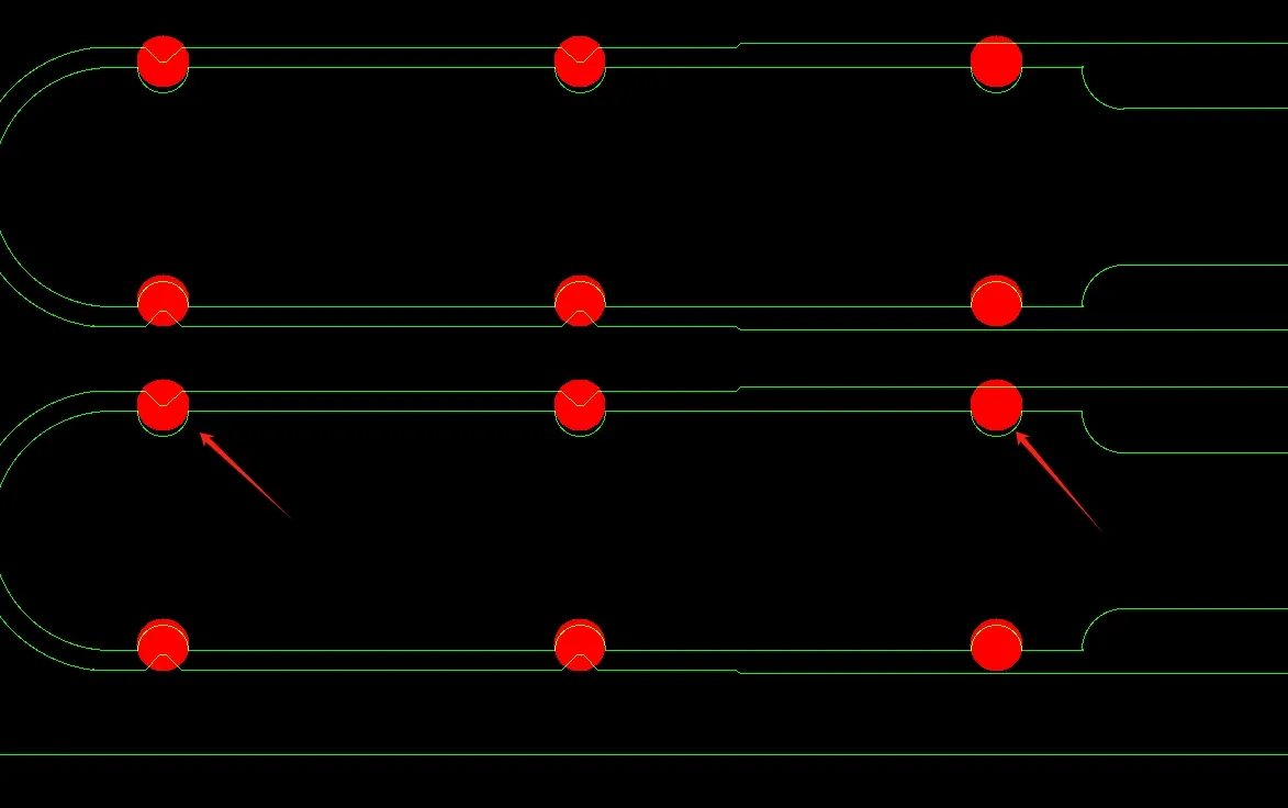
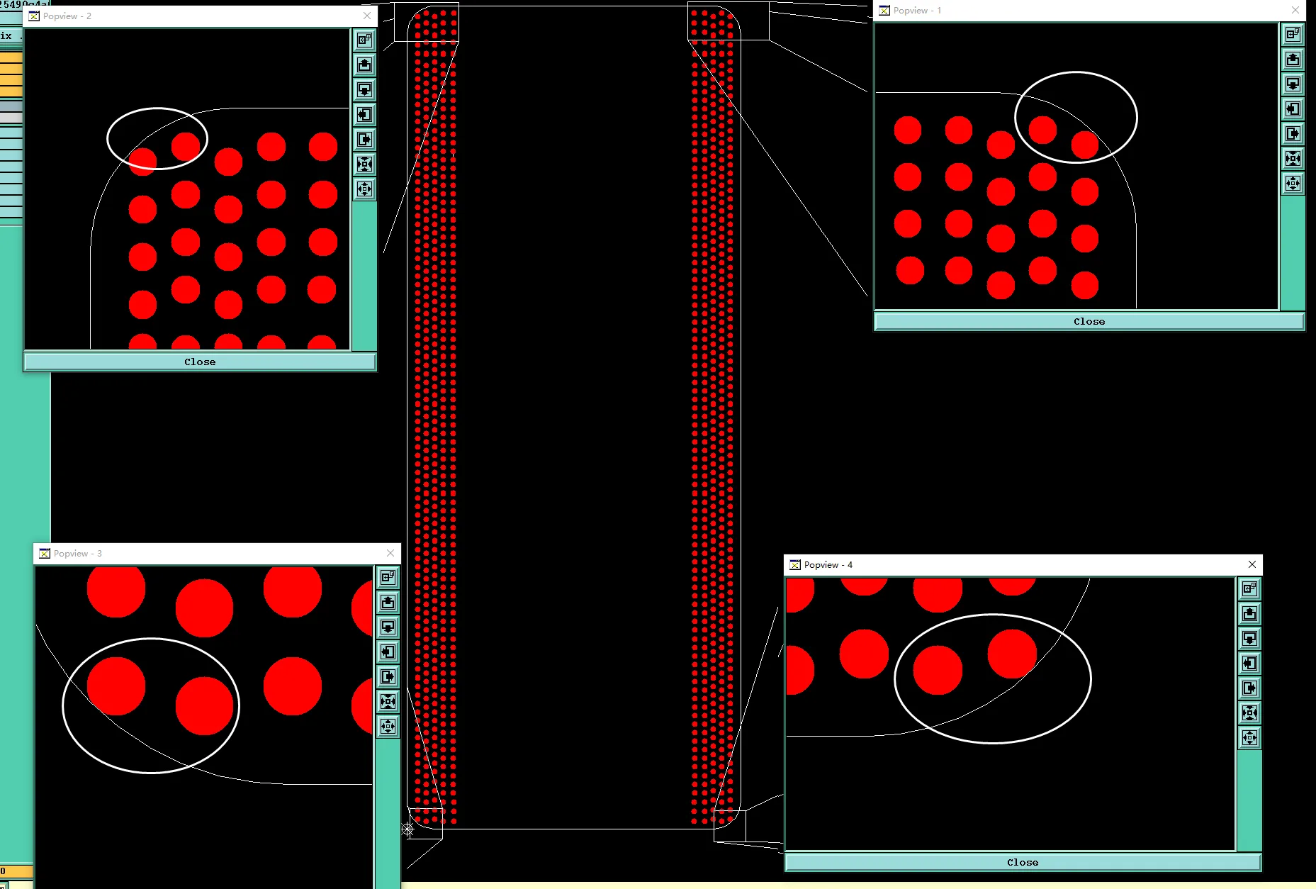
During final CAM review of a production PCB order, our engineering team identified a clear and consequential conflict between the system order parameters and the customer-supplied Gerber data. The system required via cover oil (tenting) across the board, yet the design files showed open windows at the locations marked by arrows. This tented via vs open via discrepancy created an interpretation gap that made it impossible to generate a single authoritative solder mask without risking deviation from the customer's true intent. Supporting questions about the addition of stamp holes in the panelization and the process method for 3.0 mm locating holes further reinforced the need for clarification before any production commitment could be made.
As the final engineering checkpoint between design files and factory manufacturing data, we examined the complete package—system parameters, Gerber solder mask layers, panelization outline, drill file, and fabrication notes—to determine whether the design could be manufactured exactly as intended. The primary investigation centered on the selective mismatch in via treatment, because an incorrect decision at this stage would affect every subsequent process step from solder mask generation through surface finish and final assembly compatibility.
Apparent Design Intent for Via Protection and Accessibility
The order ( #FR4-20260616-041 ) parameters indicated a conventional board construction with standard surface finish processing. System notes explicitly specified via cover oil, a requirement commonly used to seal via barrels against solder entry and contamination during HASL or similar finishes. At the same time, the customer Gerber files contained open windows over selected vias, indicating that the designer had deliberately left certain locations accessible. This combination suggested a design that sought both general via protection and selective functional access for testing, through-hole soldering, or other assembly needs.
Panelization followed a customer self-panel approach. The presence of 3.0 mm locating holes implied the need for accurate tooling registration during fabrication and subsequent assembly. The overall design intent therefore appeared to prioritize clean mechanical outlines, reliable tooling, and a carefully controlled via condition. However, the divergence between the global system requirement for tenting and the selective open windows in the Gerber data created an ambiguity that could not be resolved by the files alone.
Without explicit confirmation, any decision made by the CAM team would have been an assumption rather than a verified interpretation of design intent. Releasing the job under either the system default or the Gerber appearance risked producing boards whose via condition differed from what the customer expected during electrical test or final assembly.
Initial CAM Observations of the Via Coverage Mismatch
Our CAM engineer first observed the conflict while performing the standard layer-by-layer comparison of system parameters against the Gerber solder mask data. At the positions highlighted by arrows in the customer file, the design clearly showed open windows. The system order, however, required cover oil for vias. Further verification confirmed that the difference was selective rather than uniform across the entire board. Some PCB vias followed the tenting requirement while the marked locations remained open.
This tented via vs open via inconsistency immediately raised process-level concerns. Cover oil seals the via against molten solder during surface finish, protecting the barrel and preventing wicking. An open window allows solder to enter the barrel, which may be intentional for certain functional vias. Applying the wrong treatment at even a few locations would alter the electrical and mechanical behavior of those vias and could introduce variability across the panel.
| Engineering Observation | Conflict Identified | Potential Manufacturing Outcome | Recommended Action |
|---|---|---|---|
| System order requires via cover oil | Gerber shows open windows at arrow locations | Incorrect via condition after surface finish | Confirm whether tenting or opening is required |
| Panelization lacks stamp holes | Separation features incomplete | Edge damage or incomplete depanelization | Confirm addition of stamp holes per standard |
| 3.0 mm locating holes present | Process method not specified | Possible tolerance or edge quality variation | Confirm if precision routing is required |
Detailed Conflict Analysis of Selective Via Treatment
The primary design-to-manufacturing and data-to-data conflict centered on the selective mismatch between the global system requirement for via cover oil and the open windows shown in the Gerber data at specific locations. In FR4 PCB fabrication, these two treatments produce fundamentally different results during surface finish processing. Tenting (cover oil) seals the via barrel, preventing solder entry and protecting against contamination. An open window allows solder to flow into the barrel, which may be required for through-hole component soldering, in-circuit test access, or other functional purposes.
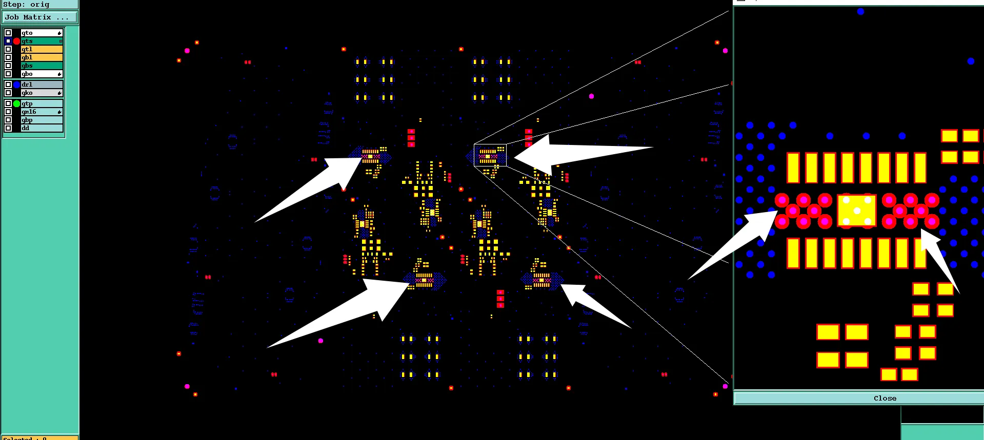
Figure 1: the customer-provided file shows an open window at the arrowed location
Because the conflict was selective rather than board-wide, the risk of inconsistent treatment was higher. A global decision to tent every via would close the intentional open windows. A global decision to leave every via open would ignore the system requirement for cover oil on the remaining vias. Either choice would produce boards that partially failed to match the customer's design intent. According to IPC-A-600 acceptability criteria for solder mask coverage and via condition, the finished via must correspond to the documented requirement. Without clarification, the engineering team lacked the confidence to generate a single correct solder mask layer set.
Realistic manufacturing consequences included solder bridging or incomplete filling on vias that should have remained open, or unprotected barrels on vias that required tenting. These outcomes could surface during electrical testing as intermittent connections or during customer assembly as soldering defects. The conflict therefore blocked production release until the customer confirmed the intended condition for the vias marked by arrows.
The presence of secondary issues reinforced the decision to hold the job. The panelization data did not include stamp holes at the connection tabs. Without stamp holes, the mechanical force required to separate the panel can concentrate at uncontrolled points, increasing the chance of edge fracture or incomplete boards. The 3.0 mm locating holes raised a process question: whether standard drilling would provide adequate positional accuracy and edge quality, or whether conversion to precision routing was necessary. These supporting concerns demonstrated that the data package still contained multiple points of ambiguity, even though the via treatment conflict remained the dominant issue affecting manufacturability.
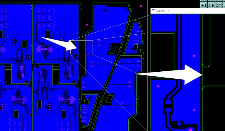
Figure 2: add the stamp holes
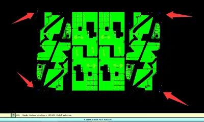
Figure 3: 3.0 mm positioning holes
Secondary Panelization and Tooling Considerations
The absence of stamp holes in the customer-supplied panelization increased the risk of uncontrolled separation. Standard process practice adds stamp holes (mouse bites) at connection tabs to define a clean break point and reduce stress on the board outline. Without them, depanelization forces can produce jagged edges or cracks that propagate into nearby copper features. The 3.0 mm locating holes required explicit confirmation of process method because larger tooling holes sometimes benefit from precision routing when tight positional tolerance or improved wall quality is needed. These secondary observations did not independently stop production, yet they confirmed that a complete resolution of all interpretation gaps was required before tooling generation.
Engineering Clarification Path and Manufacturing Decision
We issued a focused set of Engineering Questions centered on the primary conflict. The first question asked the customer to confirm whether the vias at the arrow locations should follow the system requirement for cover oil (tenting) or the open-window design shown in the Gerber files. Additional questions addressed the addition of stamp holes according to standard panelization practice and whether the 3.0 mm locating holes required conversion to a precision routing process.
Customer response clarified that the open windows at the indicated positions were intentional for functional access, while the remaining vias were to receive cover oil as specified in the system order. Stamp holes were authorized for addition at the connection tabs under standard process. The 3.0 mm locating holes were confirmed for standard drilling without conversion to precision routing. These answers provided the missing design intent and allowed the engineering team to proceed with a consistent interpretation.
Engineering then regenerated the solder mask layers to preserve the selective open windows while applying cover oil to all other vias. The panelization outline was updated to include stamp holes at the appropriate locations. The locating hole process remained under standard drilling parameters. Internal verification confirmed that the revised data set produced uniform via treatment, controlled separation features, and accurate tooling registration. Only after this validation was the job released to production with the confirmed tented via vs open via interpretation locked into the manufacturing files.
| Aspect | Before Clarification | After Resolution |
|---|---|---|
| Via Treatment at Arrow Locations | System cover oil vs Gerber open windows | Open windows confirmed as intentional |
| Panel Separation Features | No stamp holes defined | Stamp holes added per standard practice |
| 3.0 mm Locating Holes | Process method unspecified | Standard drilling confirmed |
| Overall Manufacturing Status | Engineering hold | Released to production |
Practical Design Lessons for Consistent Via Solder Mask Control
- Ensure that every via in the Gerber solder mask layers matches the treatment stated in the system order or fabrication notes.
- When selective open windows are required on an otherwise tented design, clearly identify those locations in both textual notes and graphical data so that CAM systems can interpret the intent without ambiguity.
- Confirm the addition of stamp holes early in the panelization review when using customer self-panel layouts, especially if connection tabs are present.
- Specify the preferred process method for locating holes larger than standard diameters if tighter positional accuracy or improved edge quality is needed.
- Perform a complete cross-check of system parameters against actual Gerber solder mask data before file submission to catch tented via vs open via mismatches at the design stage.
- Consider the effect of the chosen surface finish on via behavior: open vias allow solder entry while tented vias prevent it, and the choice must align with assembly and test requirements.
- Document any intentional exceptions to a global via treatment rule so that manufacturing interpretation remains consistent across the entire panel.
- Treat via solder mask coverage as a critical design attribute rather than a secondary detail that can be resolved after other features have been finalized.
Conclusion
The investigation into the tented via vs open via conflict demonstrated how a selective mismatch between system parameters and Gerber layers can halt an otherwise complete production order. By isolating the primary via treatment discrepancy, confirming secondary panelization and tooling details, and obtaining explicit customer direction, the engineering team converted an ambiguous data package into a manufacturable design. The final files supported consistent solder mask processing, controlled panel separation through the addition of stamp holes, and accurate locating features under standard process. This resolution preserved both the protective intent of cover oil on most vias and the functional accessibility of the selectively opened vias, allowing the order to proceed with the customer's true design intent fully realized in the manufacturing data.
FAQ
Q1: Why does a tented via vs open via mismatch between system order and Gerber data trigger an Engineering Question?
A1: Cover oil (tenting) and open windows produce opposite results during surface finish. Without confirmation, the manufacturer cannot decide which treatment to apply and risks producing boards that fail to match the customer's functional or reliability expectations.
Q2: What are the realistic manufacturing risks of applying the wrong via coverage?
A2: Tenting vias that should remain open can block solder access or in-circuit test probing. Leaving vias open that require protection can allow solder wicking, contamination of the barrel, or reduced long-term reliability under thermal cycling.
Q3: How should selective open windows be documented on a design that otherwise requires tenting?
A3: Explicitly identify the locations in the fabrication notes and ensure the corresponding Gerber solder mask layers show clear openings only at those positions. Graphical callouts combined with textual description prevent interpretation errors.
Q4: Why is the addition of stamp holes confirmed during panelization review?
A4: Stamp holes define a controlled break point during depanelization. Without them, separation forces can create jagged edges, incomplete boards, or cracks that propagate into functional copper features.
Q5: When might 3.0 mm locating holes require a change to precision routing?
A5: When tighter positional accuracy or improved hole-wall quality is needed for tooling registration. Confirmation ensures the chosen process matches the design's tolerance and edge-condition expectations.
Q6: What is the most effective method to prevent tented via vs open via conflicts before file submission?
A6: Generate the solder mask layers from the same source data used for the fabrication notes, perform a complete visual cross-check of every via, and maintain consistent terminology (cover oil/tenting versus open window) across all documentation.