02:50
02:50
Via Design
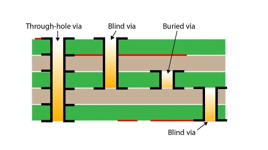
Via design plays a critical role in printed circuit board (PCB) engineering, serving as the essential pathways that connect multiple layers within a board. These conductive holes, or vias, enable efficient signal routing, power distribution, and thermal management in complex electronic assemblies. For engineers and hobbyists searching for via design resources, this tag aggregates articles that delve into the fundamentals and advanced techniques, helping you optimize your PCB layouts for reliability and performance. Understanding via design begins with selecting the appropriate type, such as through-hole, blind, or buried vias, each suited to specific applications like high-density interconnects or space-constrained designs. Practical best practices include calculating via size and aspect ratio to minimize resistance and inductance, ensuring proper annular ring dimensions to prevent manufacturing defects, and incorporating via stitching for improved grounding in high-frequency circuits. These strategies are particularly valuable for mitigating issues like signal crosstalk or electromagnetic interference in modern electronics, from consumer gadgets to industrial systems. By exploring the content under this via design tag, you can access detailed guides on simulation tools, fabrication constraints, and real-world case studies that demonstrate how effective via implementation enhances board durability and functionality. Whether you are troubleshooting a prototype or scaling up production, these resources offer actionable steps to refine your designs and avoid common pitfalls in PCB development.
Video Guide

Technical Articles

The "Black Hole" on Pads: Why Via-in-Pad Must Be Filled or Avoided
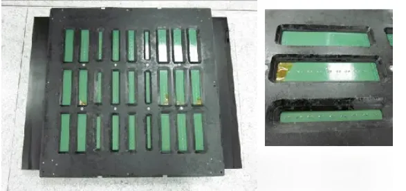
Improving DIP Solder Fill: A DOE on Thermal Relief Pads and PTH Clearance
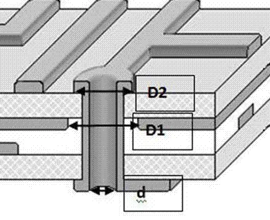
Why High-Speed PCB Traces Should Not Use Too Many Vias
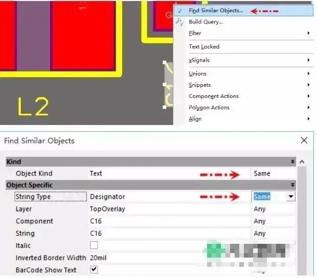
Global Editing Techniques in Altium Designer (Find Similar Objects)

Common PCB Design Pitfalls and How to Avoid Them

Adding Via Stitching in KiCad with the kicad-action-scripts Plugin

Precise Spacing Control: How to Move a Diagonal Feature by Exactly 1 mm
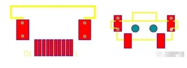
Via Design Guidelines in PCB Design: Balancing Performance and Cost
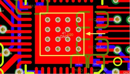
Can You Place a Via on a Pad?
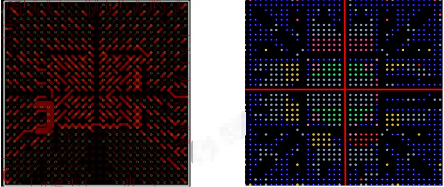
PCB Via Fanout Details That Are Easy to Miss
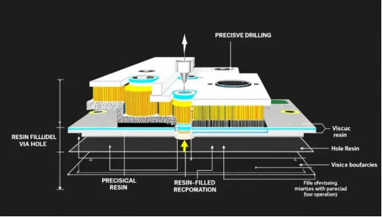
Which Vias Need Resin Plugging? Real Engineer Questions from Production
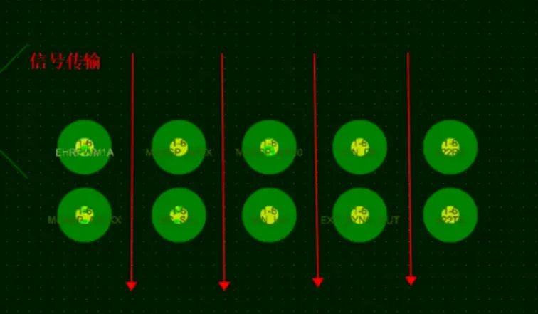
High-Speed PCB Vias: A Small Feature That Can Break the Signal
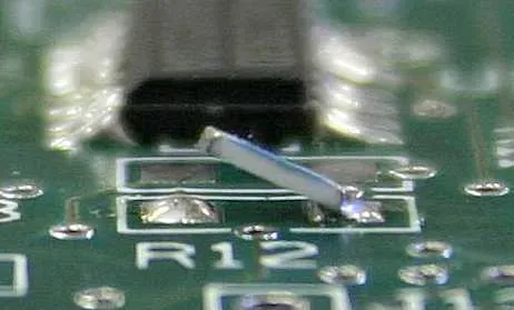
Can a Via Be Placed in a Pad? A Detail PCB Designers Cannot Skip
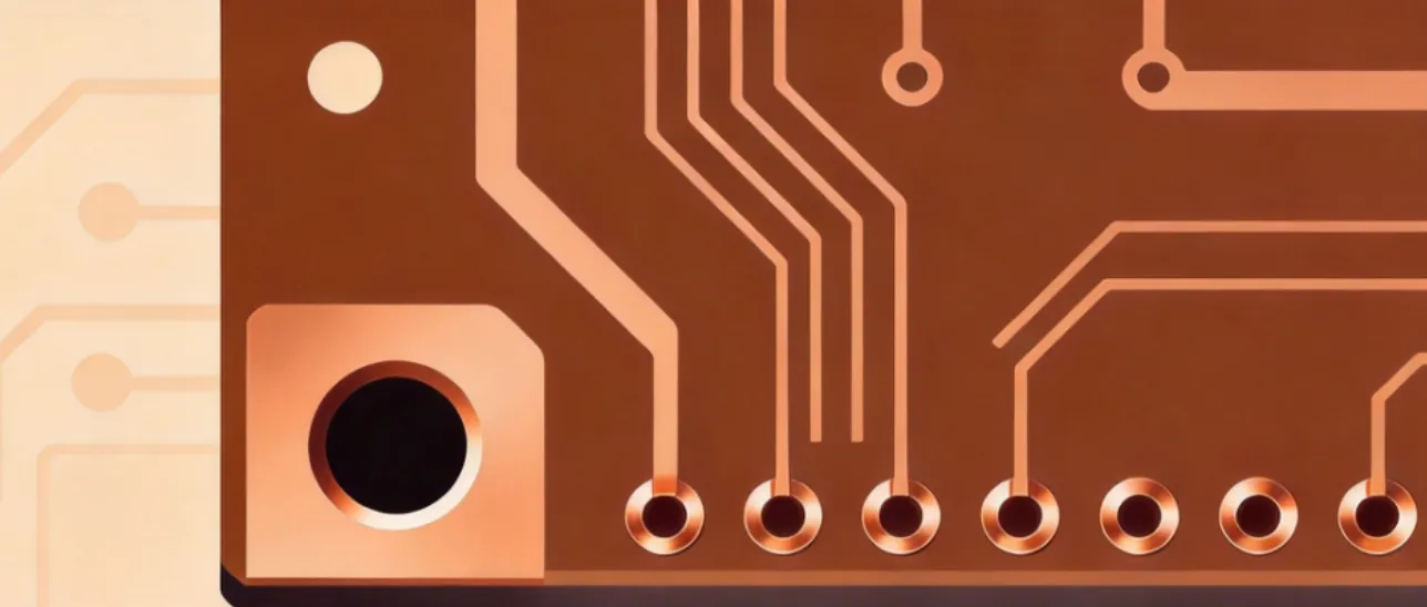
How to Reduce Via Parasitic Inductance in High-Speed Routing

Why Traces Can Still Open After Teardrops Are Added to Vias
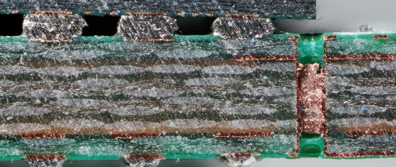
Small Anti-Pads Can Cause Unconnected Vias to Short

Should a PCB Via Be Tented or Exposed? Do Not Select the Wrong Option by Habit
Mastering Hand-Soldering on Blind Via PCBs: A Hobbyist's Guide
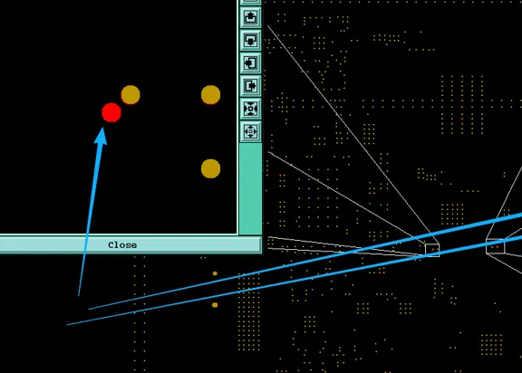
PCB CAM Review: Fix V-Cut & Via Spacing to Avoid Delays