In the world of rigid-flex PCB production, even well-prepared Gerber files often require detailed engineering review. This case study examines a real 4-layer rigid-flex order that we processed recently. The design combined a 0.6mm rigid section with a 0.15mm flex area, ENIG surface finish, 4mil line/space, and tight mechanical constraints.
During our standard CAM engineering review, we identified several manufacturability issues typical of rigid-flex constructions. These issues, if left unaddressed, could have led to serious production problems including delamination at the rigid-flex interface, chemical contamination of inner layers, and mechanical failure during depanelization. This article details what we found, why we raised EQs, and how we resolved them to ensure reliable production.
4-Layer Rigid-Flex PCB Order Specifications and Stackup
This was a compact 4-layer rigid-flex PCB (#RFP-20260312-007) measuring 46mm × 16mm per unit, with a 2×2 panelization arrangement resulting in a 106mm × 46mm panel. The customer ordered 20pcs (5 sets). The stackup featured a 0.6mm ±0.1mm rigid section and 0.15mm ±0.05mm flex section. Surface finish was ENIG with 1.0μm minimum gold thickness. Minimum hole size was 0.2mm, with impedance requirements specified.
The rigid portion used double-sided green solder mask with white legend, while the flex area specified single-sided yellow coverlay on the bottom. Inner layer copper was 18μm, outer layer 35μm. The design included flying probe testing and specific panelization requirements. This combination of tight tolerances, hybrid construction, and small panel size made it a classic case requiring careful DFM validation before production release.
Critical Issues Found During Rigid-Flex PCB CAM Review
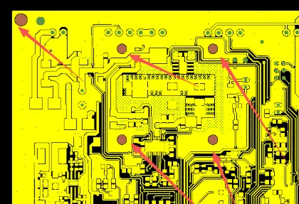
1. Sharp Internal Right Angles at Rigid-Flex Transition Zone
One of the first issues our CAM engineer flagged was the presence of sharp internal right angles in the hard board area near the rigid-flex transition zone. In rigid-flex PCB manufacturing, these sharp corners create high stress concentration points during flexing and lamination.

Figure 1: Sharp internal right angles in the hard board area
We noticed that maintaining these sharp internal corners would be extremely difficult to achieve consistently in production and could lead to tearing at the material interface. Our engineer suggested modifying the internal corners to a 0.5mm radius (R0.5). This change helps distribute mechanical stress more evenly and reduces the risk of material separation during the pressing process and subsequent handling.
If this issue had been ignored, the panels could have suffered from delamination or cracking at the junction during depanelization or in-field flexing, leading to open circuits or complete board failure. According to typical IPC-2221 guidelines for flexible circuit transitions, generous radii are recommended to maintain structural integrity.
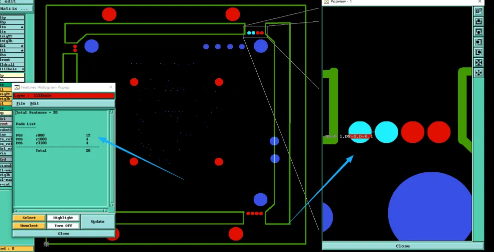
2. Insufficient Via Clearance to Flex Outline
Another critical finding involved several through-holes located too close to the flex outline — less than 0.6mm in some areas. In rigid-flex boards, this proximity creates a significant risk during wet processes (desmear, plating, and surface finish), where chemicals can wick into the inner layers through the flex-rigid boundary.

Figure 2: Several through-holes located too close to the flex outline
To mitigate this, we relocated affected vias to maintain a minimum 0.6mm distance from the flex outline. This adjustment was necessary to protect the inner copper layers from contamination that could cause plating voids, resin voids, or delamination.
Had we proceeded without this change, the boards risked catastrophic inner layer damage during ENIG processing, potentially resulting in scrap rates exceeding 50% and unreliable electrical performance due to compromised via reliability.
3. Stackup Thickness and Copper Weight Conflicts
The customer documentation showed conflicting thickness requirements: one file called for 0.8mm rigid thickness while the order email specified 0.6mm. Additionally, with the flex material on the outer layers, we recommended adjusting inner layer copper to ½ oz (18μm) to better match the flex copper weight and reduce the risk of uneven stress during lamination.

Figure 3: 0.8mm rigid thickness in the file
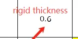
Figure 4: Specified 0.6mm in the order email
After reviewing the full stackup (hard board 0.6mm ±0.1mm, flex 0.15mm ±0.05mm), we confirmed production would follow the email specification of 0.6mm and adjusted impedance data accordingly.

Figure 5: Rigid thickness and flex thickness data
Mismatched stackup data is a common source of warpage and impedance deviation in rigid-flex boards. Proceeding with inconsistency could have caused significant board warpage, impedance mismatch, and assembly issues downstream.
4. Panelization, Solder Mask, and Silkscreen Optimization
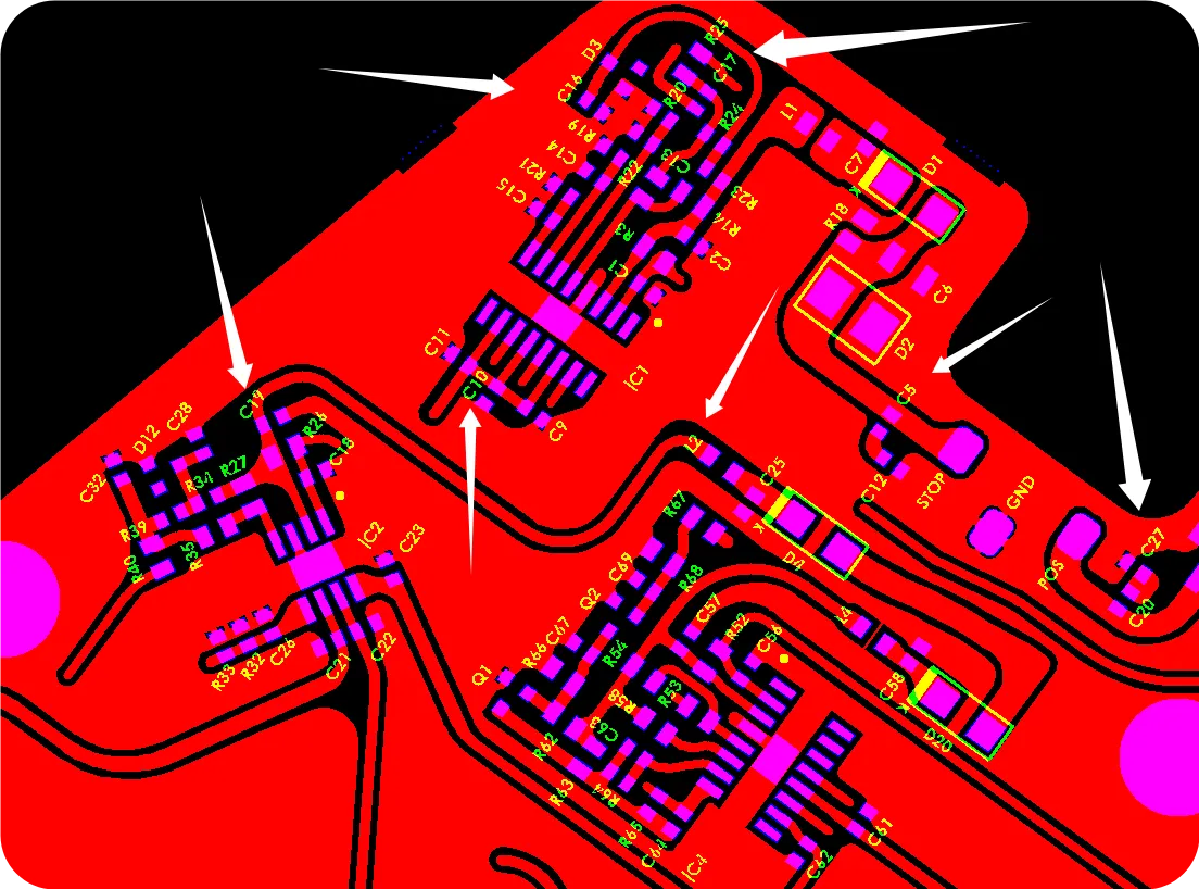
We applied standard rigid-flex panelization: milling slots, stamp holes, positioning holes, optical fiducials, and grid copper on process edges. The customer requested a 55mm process edge width, which we confirmed. Silkscreen optimization was also performed — moving characters where possible and removing those directly on pads to prevent solderability issues.
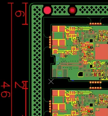
Figure 6: Rigid-flex panelization
Figure 7: Before characters-removing

Figure 8: After characters-removing
In the dense pad area, the spacing was insufficient for a reliable solder mask bridge. We recommended opening the solder mask window to avoid mask residue or bridging defects during assembly.
Without these adjustments, we could have seen poor legend adhesion, solder mask peeling, or shorts during PCB SMT assembly.
Key DFM Challenges in Rigid-Flex PCB Designs
This case highlights several recurring challenges in rigid-flex design:
- Sharp geometry at material transitions increases tearing risk during fabrication and use.
- Insufficient clearance between vias and flex boundaries invites chemical contamination.
- Conflicting documentation between files and emails leads to production delays.
- Tight pad spacing often requires solder mask window adjustments for reliable yield.
Each of these issues, if ignored, could result in hole breakout, copper peeling, via cracking, or complete panel scrap. Early CAM review prevents these outcomes and reduces the need for multiple revision cycles.
| Issue | Risk if Unresolved | Adjustment Made |
|---|---|---|
| Sharp Transition Corners | Tearing or delamination | Added R0.5 radius |
| Via-to-Flex Clearance | Chemical contamination | Relocated vias to ≥0.6mm |
| Stackup Conflicts | Warpage and impedance errors | Locked 0.6mm per email spec |
| Tight Pad Spacing | Mask bridging or shorts | Opened solder mask windows |
Table 1: Major Rigid-Flex DFM Issues Identified
Collaborative Resolution of Rigid-Flex EQs
Our team worked closely with the customer to provide annotated images for every suggestion. All major changes were documented and confirmed before finalizing the production data. The stackup was locked, impedance values recalculated, and panelization optimized for maximum usable yield within the 2 X-board tolerance per set.
By addressing these points proactively, we protected both mechanical reliability at the rigid-flex junction and electrical integrity throughout the board.
Successful Production After DFM Adjustments
All engineering questions were resolved and confirmed by the customer. Production data was updated, CAM files approved, and the order successfully released for fabrication under IPC-6012 Class 2 standards with enhanced DFM measures in place.
DFM Best Practices for Rigid-Flex PCB Designs
- Always provide consistent thickness specifications across all documents for rigid-flex designs.
- Include adequate radii (minimum R0.5) at rigid-flex transition corners.
- Maintain at least 0.6mm clearance between vias and flex boundaries.
- Define solder mask requirements clearly in dense BGA or fine-pitch areas.
- Specify copper weights carefully when flex material is on outer layers.
- Provide complete panelization intent early to avoid last-minute adjustments.
- Use proper layer naming and fabrication notes to reduce miscommunication.
FAQ
Q1: Why is via-to-flex outline clearance so important in rigid-flex PCBs?
A1: Insufficient clearance allows plating and etching chemicals to penetrate the interface layers, causing contamination, voids, or delamination that can lead to board scrap.
Q2: Can sharp internal corners be used at rigid-flex junctions?
A2: Generally no. They create stress risers that increase the likelihood of tearing or cracking during lamination and mechanical handling. A minimum R0.5 is strongly recommended.
Q3: Why do factories sometimes remove or move silkscreen markings?
A3: Markings directly on SMT pads can interfere with solder paste application and reflow, leading to poor solder joints or tombstoning. We optimize to maintain legibility while protecting assembly yield.
Q4: What happens if stackup thickness conflicts are not resolved before production?
A4: It can cause incorrect material selection, impedance deviation, excessive warpage, and potential rejection during final inspection or assembly.
Q5: Why adjust solder mask in areas with tight pad spacing?
A5: When spacing is below reliable bridge width (typically <0.1-0.15mm depending on process), attempting to keep mask can cause incomplete openings or mask slivers, resulting in shorts or opens during assembly.