Introduction
Vias form the backbone of multilayer PCB interconnects, enabling signals to transition between layers in high-speed designs. In environments exceeding several gigahertz, these transitions introduce impedance discontinuities that degrade signal integrity. Key challenges include reflections, crosstalk, and attenuation, all exacerbated by poor via geometry. Optimizing the via aspect ratio proves crucial, as it balances manufacturability with electrical performance. This guide delves into via aspect ratio signal integrity, high-speed PCB via design principles, and strategies to mitigate parasitic inductance via and via capacitance effects. Engineers can achieve robust designs by understanding these fundamentals and applying structured best practices.
High-speed signals demand precise control over every element in the signal path. Vias, often overlooked, contribute significantly to overall insertion loss and return loss. As data rates climb, even minor parasitics become dominant. This article provides logical explanations, technical mechanisms, and actionable guidance tailored for electric engineers tackling complex PCB layouts.
What Is Via Aspect Ratio and Why It Matters for Signal Integrity
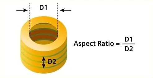
Via aspect ratio defines the ratio of the total board thickness to the finished via hole diameter, typically expressed as thickness divided by diameter. A higher ratio indicates a longer, narrower via barrel relative to the board stackup. Manufacturers prefer ratios below 10:1 to ensure uniform plating and avoid plating voids during fabrication. Exceeding this threshold risks incomplete copper deposition, leading to reliability failures under thermal stress.
For signal integrity, aspect ratio directly influences parasitic elements. Longer vias, corresponding to higher ratios, amplify inductance, which slows rise times and introduces delays. In high-speed PCB via design, this manifests as eye diagram closure and increased bit error rates. According to IPC-2221, designers should target a maximum aspect ratio of 8:1 for plated through holes to maintain both mechanical integrity and electrical performance. Balancing this parameter early prevents costly respins and ensures compliance with performance specs.
Aspect ratio also ties into layer count and material choices. Thicker stackups for power integrity often force compromises unless via strategies evolve. Engineers must evaluate trade-offs between routing density and signal quality from the outset.
Technical Principles: Parasitic Inductance and Capacitance in Vias
Parasitic inductance via arises primarily from the via barrel's length and diameter, modeled approximately as inductance proportional to height and inversely to radius. In high-speed signals, this inductance forms an LC network with surrounding structures, causing resonance peaks that distort waveforms. Stub effects from unused via portions further worsen return loss, especially when stubs extend beyond the signal layer. Minimizing via length through optimal aspect ratios reduces these parasitics effectively.
Via capacitance effects stem from the electric field coupling between the via barrel and nearby reference planes. Closer planes increase capacitance, leading to impedance drops and signal broadening. At frequencies above 1 GHz, these effects couple with inductance to create mismatches, amplifying crosstalk between adjacent vias. Engineers observe this in time-domain reflectometry as step response anomalies.
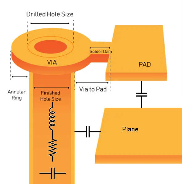
Impedance discontinuity at the via transition compounds these issues. The via's characteristic impedance differs from traces due to geometry changes, generating reflections per transmission line theory. High aspect ratios exacerbate this by prolonging the discontinuity region. Structured analysis using field solvers reveals how aspect ratio tweaks can align via impedance closer to 50 ohms or 100 ohms differential.
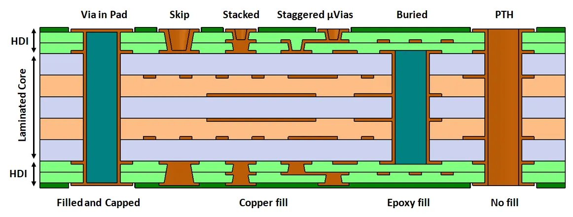
Comparing Via Types: Microvia vs Buried Via for Signal Integrity
Through vias span the entire board thickness, offering simplicity but suffering from long stubs that radiate and reflect signals. Buried vias connect only inner layers, eliminating surface stubs and reducing effective length for better via aspect ratio signal integrity. They suit mid-layer routing in dense designs, minimizing exposure to outer layer noise.
Microvias, with diameters under 150 microns, enable high-density interconnects in HDI boards. Their small size yields low parasitics, ideal for frequencies beyond 10 Gbps where microvia vs buried via signal integrity shines through shorter paths and reduced capacitance. Laser-drilled microvias support aspect ratios as low as 1:1, far superior to mechanical drills. However, they demand sequential lamination processes, increasing complexity.
Blind vias bridge surface to inner layers, offering a middle ground with controlled stub lengths. In comparisons, microvias excel in pin density, while buried vias prioritize cost for non-surface nets. Selection hinges on stackup, speed, and fab capabilities. Hybrid stacks combining types optimize overall performance.
- Through Via: Typical aspect ratio up to 8:1; strengths: simple fabrication; drawbacks: long stubs and high parasitics.
- Buried Via: Typical aspect ratio 4:1 to 6:1; strengths: no surface stubs; drawbacks: limited to inner layers.
- Microvia: Typical aspect ratio 0.5:1 to 3:1; strengths: low inductance and high density; drawbacks: higher cost and potential reliability concerns.
- Blind Via: Typical aspect ratio 3:1 to 5:1; strengths: reduced stub length; drawbacks: partial surface access only.
This list summarizes trade-offs for high-speed PCB via design.
Practical Solutions and Best Practices for Optimizing Via Aspect Ratios
Start with stackup planning to minimize board thickness for critical nets, directly lowering aspect ratios. Group high-speed signals on fewer layers to favor blind or buried vias over through types. Target finished via diameters of at least 0.2 mm to support plating while keeping ratios under 6:1 where possible.
Backdrilling removes unused stub lengths from through vias, effectively shortening the electrical path without HDI costs. This technique restores signal integrity for legacy through vias in thick boards. Pair it with optimized drill sizes to balance mechanical drill limits.
For differential pairs, use symmetric via pairs with equal aspect ratios to preserve balance. Add ground vias nearby for return path integrity, forming via fences that suppress crosstalk. Simulate parasitics early to quantify improvements.
IPC-6012 specifies qualification tests for vias under thermal cycling, ensuring designs withstand real-world stresses. Adhere to these for high-reliability applications.
Employ filled or plugged vias in BGA areas to prevent solder wicking and maintain planarity. These also reduce capacitance by filling the barrel.
Troubleshooting Common Via-Related Signal Integrity Issues
Engineers often encounter eye closure from excessive via inductance in initial prototypes. Verify aspect ratios against fab DFM reports first. If stubs persist, prioritize backdrilling for through vias on fast nets.
Crosstalk spikes indicate inadequate spacing; increase via-to-via pitch beyond minimums. Capacitance mismatches show as low-frequency droop, resolvable by plane cutouts or wider antipads.
Layer transitions demand teardrops for trace-to-via junctions to avoid etch breakout. Systematic checks align designs with standards.
Conclusion
Mastering via aspect ratio signal integrity unlocks reliable high-speed PCB performance. By prioritizing low ratios, selecting appropriate via types, and mitigating parasitics, engineers minimize discontinuities. Parasitic inductance via and via capacitance effects diminish with shorter, wider vias and advanced techniques like backdrilling. Microvia vs buried via signal integrity favors density needs, always balanced against cost. Implement these principles alongside IPC guidelines for optimal results. Future designs will leverage even tighter geometries as speeds rise.
FAQs
Q1: What is the optimal via aspect ratio for signal integrity in high-speed PCBs?
A1: Target ratios below 6:1 for critical nets to limit inductance and stubs. IPC-2221 advises no more than 8:1 for manufacturability. Thinner stackups or blind vias further improve performance by shortening effective length. Simulate to confirm impedance continuity.
Q2: How does parasitic inductance via impact high-speed signals?
A2: It introduces series inductance that slows rise times and causes ringing. Longer vias from high aspect ratios worsen this, leading to ISI and reflections. Mitigate with backdrilling or microvias for shorter paths. Ground stitching aids return currents.
Q3: What are via capacitance effects in PCB design?
A3: Capacitance forms between via barrels and planes, dropping impedance and broadening pulses. Tight coupling increases it, affecting low frequencies. Widen antipads or use buried vias to reduce coupling. Balance with inductance for flat response.
Q4: In microvia vs buried via signal integrity, which is better for 10 Gbps+?
A4: Microvias offer superior parasitics due to small size and short lengths, ideal for HDI. Buried vias suit inner routing with good stub control at lower cost. Choose based on layer access; hybrids often best.
References
IPC-2221B — Generic Standard on the Design of Rigid and Electronic Circuits. IPC, 2009
IPC-6012E — Qualification and Performance Specification for Rigid Printed Boards. IPC, 2017
IPC-A-600K — Acceptability of Printed Boards. IPC, 2020


