Introduction
This engineering case examines a 6-layer FR-4 PCB order (#FR4-20260429-022) that presented several manufacturability challenges during our standard CAM review process. With dimensions of 80 × 200 mm, 2.0 mm finished thickness, 1 oz copper on outer layers, and lead-free HASL surface finish, the design was intended for standard digital applications. However, the combination of small 0.2 mm vias, tight 3 mil trace/space, mixed plated and non-plated holes, and specific solder mask requirements created multiple points where design intent met manufacturing constraints.
In our experience as CAM engineers, 6-layer boards in this thickness range frequently trigger engineering questions (EQs) around via tenting, solder mask consistency, non-plated hole handling, and panelization. We always perform a thorough DFM analysis before releasing files to production to prevent scrap, delays, and field failures. This case highlights the key issues we identified, the risks involved, and how clarification with the customer led to a manufacturable production package.
Order Overview
The PCB is a 6-layer rigid board using FR-4 TG150 material with 2.0 mm overall thickness. Outer copper weight is 1 oz, inner layers also 1 oz. Minimum hole size is 0.2 mm, with line width/space at 3 mil. The board requires 100% flying probe testing, lead-free HASL surface finish, green solder mask on both sides, and white silkscreen. Quantity is 25 pieces (single panel 1×1 configuration). Delivery target was 13 days. The stackup followed a standard symmetrical configuration with no special impedance requirements noted. Panelization was simple, but several file-level inconsistencies required attention before mechanical routing and plating processes.
Main Engineering Questions Found During CAM Review
Via Tenting and Solder Mask Opening Conflicts
One of the first issues our CAM team identified was a mismatch between the fabrication notes and the actual Gerber data regarding via coverage. The order specified via tenting (cover with solder mask), yet multiple vias in the provided files had explicit solder mask openings. We noticed this discrepancy immediately during drill and mask layer comparison.
Figure 1: Explicit solder mask openings on vias
Our engineer suggested removing the solder mask openings on vias and processing them with ink tenting to prevent solder intrusion. If ignored, vias on a HASL board would likely trap solder beads inside the holes, leading to potential short circuits during assembly or cosmetic defects that fail IPC-A-600 visual inspection. In worse cases, excess solder could cause via cracking under thermal stress or unreliable electrical contact. After customer clarification that they preferred no ink plugging due to process concerns, we documented acceptance of possible tin beads with a manufacturing note.
Figure 2: Suggested ink tenting to prevent solder intrusion
Non-Plated Hole Annular Ring and Pad Clearance Issues
Several non-plated holes showed extremely tight or insufficient annular rings relative to the surrounding copper. Our CAM engineer confirmed that the mechanical drill tolerance and etching process would make reliable isolation impossible without modification. We therefore proposed deleting the corresponding pads and traces around these non-plated holes to ensure clean mechanical drilling without copper remnants.
Figure 3: Tight non-plated hole annular ring
If production had proceeded without this change, the result could have been partial copper breakout, exposed copper edges, or shorting between non-plated holes and adjacent circuitry. This is a common risk in mixed-hole designs and aligns with IPC-6012 Class 2 minimum annular ring requirements for mechanical holes. The customer accepted our proposed data modification after review of the highlighted areas.
Silkscreen Overlapping Solder Mask Openings
Silkscreen characters were placed directly on or overlapping solder mask openings for component pads. The character width was also relatively tight for the chosen silkscreen process. To prevent ink adhesion issues on exposed copper pads, we recommended removing both the characters and their bounding boxes from the mask openings (similar to the highlighted pink regions in our review markup).
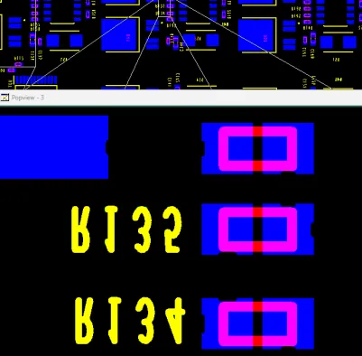
Figure 4: Silkscreen characters were placed directly on or overlapping solder mask openings
Without adjustment, silkscreen ink on pads could cause poor solderability, component placement misalignment, or visual inspection failures. Our team has seen this lead to assembly rework or even scrapped boards when ink contamination affects reflow. The customer confirmed the removal.
Vias Overlapping or Too Close to Large Holes
Highlighted vias were positioned too close to or overlapping larger drilled holes. Our engineer suggested deleting the conflicting vias to maintain structural integrity and plating reliability during the drilling sequence. Proceeding without correction risked drill wander, breakout, or plating voids at the intersection points.
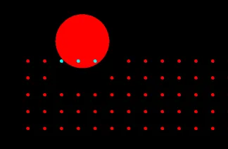
Figure 5: Highlighted vias are positioned too close to or overlapping larger drilled holes.
Board Thickness and Stackup Clarification
A minor but important note was a potential finished thickness conflict between the specified 2.0 mm and the calculated stackup. We verified the dielectric materials and copper weights to ensure compliance before lamination.
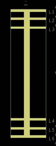
Figure 6: Board thickness and stackup info
Suggested EQ Categories
File & Manufacturing Data Issues
- Solder mask opening conflicts on vias
- Silkscreen placement over pads
- Non-plated hole pad definitions
Hole & Tolerance Issues
- Via proximity to large holes
- Insufficient annular rings on non-plated holes
Panelization & Process Optimization
- Confirmation of 1×1 panelization suitability
- V-CUT and routing clearance verification
Manufacturing Risks and DFM Insights
This case underscores several recurring DFM pitfalls in multi-layer designs. Tight via placement near larger holes often stems from layout congestion but ignores drill sequencing realities. Without clarification, this can cause registration errors and yield loss exceeding 20% in small runs. Similarly, mismatched via tenting expectations frequently lead to post-HASL cleaning issues or assembly defects.
Non-plated hole handling is another area where designers sometimes underestimate etching and drilling tolerances. If left unaddressed, it risks copper slivers or incomplete isolation, resulting in open circuits or intermittent failures in the field. Our review process caught these before production, avoiding potential full lot scrap and schedule slippage.
How the Engineering Team Resolved the Issues
We compiled all marked-up issues into a single EQ package with annotated Gerbers and sent it to the customer for confirmation. For the via tenting conflict, after discussion we documented acceptance of possible tin beads rather than forcing ink plugging. Non-plated hole pads were removed as proposed. Silkscreen cleanup was applied per standard practice.
Our CAM engineer also verified panelization layout for proper routing and V-CUT margins. Once all confirmations were received and updated files reviewed, we proceeded with data preparation, including netlist comparison and DRC validation.
Final Manufacturing Outcome
All engineering questions were resolved through clear customer feedback and targeted data adjustments. The finalized production package met both design intent and manufacturing capabilities. The order was released for fabrication with standard process controls, including 100% flying probe electrical test. No further revisions were required.
Key Takeaways for PCB Designers
- Always clearly specify via tenting or plugging requirements in fabrication notes and ensure consistency with mask layers.
- Avoid placing silkscreen legends over exposed copper pads; maintain adequate clearance.
- For non-plated holes, verify annular ring and isolation in the design software against actual manufacturing tolerances.
- Provide complete stackup details early to prevent thickness mismatches.
- Review Gerber files for layer alignment before submission, especially drill and mask layers.
- Consider panelization early if V-CUT or scoring is involved to maintain adequate clearances.
FAQ
Q1: Why do PCB factories require confirmation on via tenting for HASL boards?
A1: HASL process floods holes with molten solder. Untented vias easily trap solder beads, causing assembly issues or visual defects. Tenting reduces this risk but must be balanced with customer process needs.
Q2: What happens if non-plated hole annular rings are too small?
A2: Etching and drill tolerances can remove isolation, leaving copper slivers or shorts. Deleting pads is a common safe resolution to guarantee clean mechanical holes.
Q3: Why remove silkscreen from solder mask openings?
A3: Silkscreen ink on exposed pads interferes with soldering, leading to weak joints or component misalignment. Standard DFM practice is to clear legends from all openings.
Q4: How does CAM review prevent board thickness conflicts?
A4: Engineers calculate pressed thickness from the exact stackup materials and copper weights, then compare against customer specification. Adjustments to dielectrics or prepreg can be made if needed.
Q5: Is it normal for vias to be deleted during review?
A5: Yes, when they conflict with larger holes or violate minimum spacing for reliable plating. Deletion prevents breakout and maintains yield.