02:50
02:50
Via Design
Via design plays a critical role in printed circuit board (PCB) engineering, serving as the essential pathways that connect multiple layers within a board. These conductive holes, or vias, enable efficient signal routing, power distribution, and thermal management in complex electronic assemblies. For engineers and hobbyists searching for via design resources, this tag aggregates articles that delve into the fundamentals and advanced techniques, helping you optimize your PCB layouts for reliability and performance. Understanding via design begins with selecting the appropriate type, such as through-hole, blind, or buried vias, each suited to specific applications like high-density interconnects or space-constrained designs. Practical best practices include calculating via size and aspect ratio to minimize resistance and inductance, ensuring proper annular ring dimensions to prevent manufacturing defects, and incorporating via stitching for improved grounding in high-frequency circuits. These strategies are particularly valuable for mitigating issues like signal crosstalk or electromagnetic interference in modern electronics, from consumer gadgets to industrial systems. By exploring the content under this via design tag, you can access detailed guides on simulation tools, fabrication constraints, and real-world case studies that demonstrate how effective via implementation enhances board durability and functionality. Whether you are troubleshooting a prototype or scaling up production, these resources offer actionable steps to refine your designs and avoid common pitfalls in PCB development.
Video Guide


Technical Articles
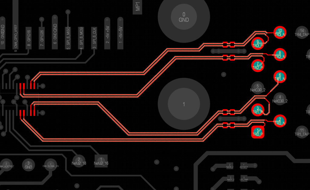
Via Placement for Differential Pairs: Maintaining Impedance and Signal Integrity
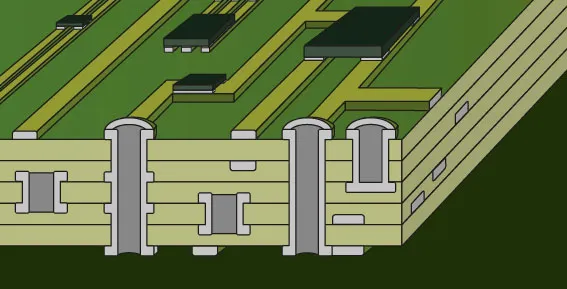
Blind Via Design Rules
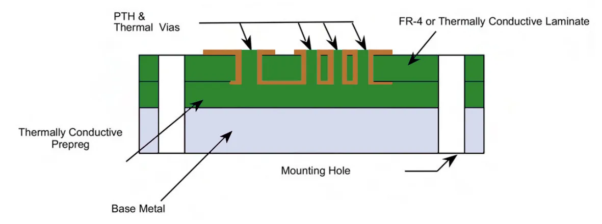
Aluminum PCB Thermal Vias: Design Rules and Best Practices
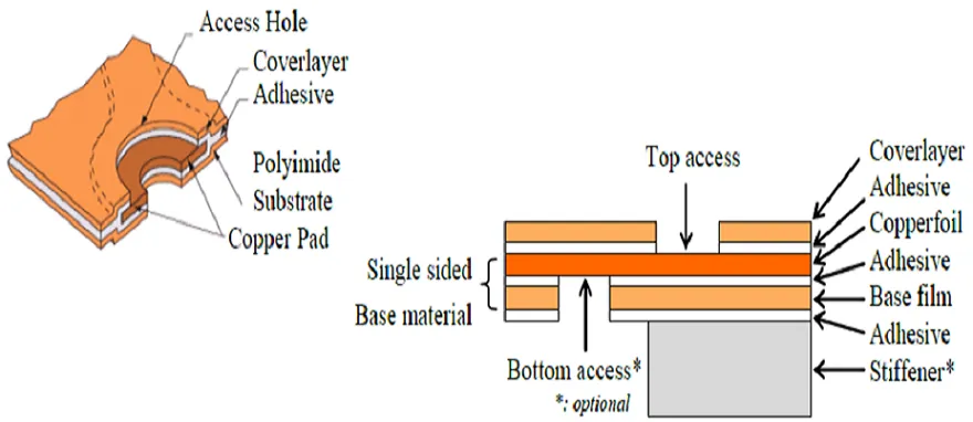
Polyimide PCB Thermal Vias: Enhancing Heat Dissipation in Flexible Designs
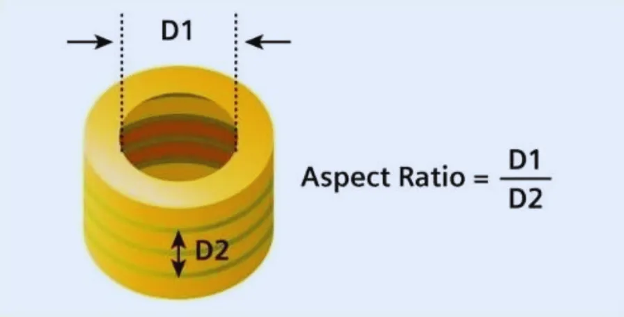
Ensuring PCB Reliability: The Crucial Role of Via Aspect Ratio
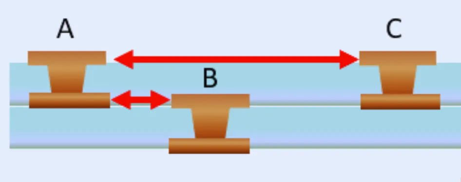
Optimizing Via Spacing for Enhanced Signal Integrity in High-Speed PCBs
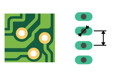
Optimizing Plated Through-Hole Design for High-Speed PCB Performance
Through-Hole Vias: Essential Connections in Multilayer PCB Design
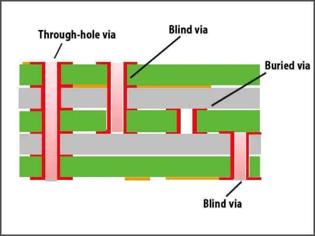
Blind Vias in PCB Design: Optimizing High-Density Boards
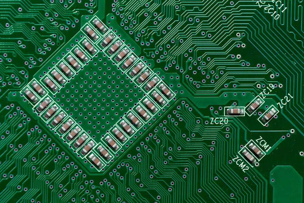
Exploring the World of Multilayer FR-4 PCBs: Design, Manufacturing, and Applications
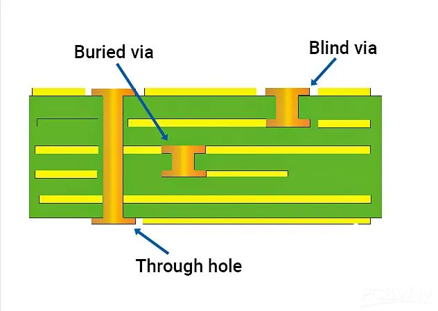
FR 4 PCB Vias: Types, Design Rules, and Manufacturing Considerations
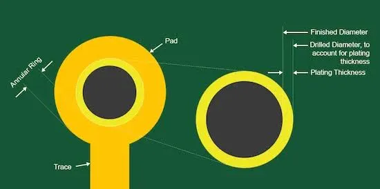
FR4 PCB Via Size and Pad Size: How to Choose the Right Dimensions
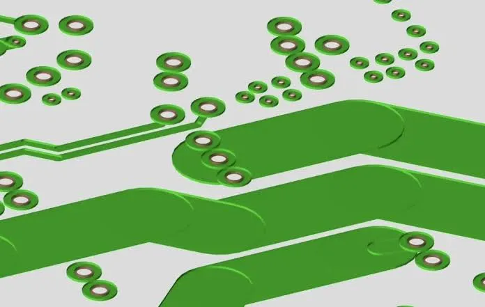
FR4 PCB Stitching Vias: When and Where to Use Them
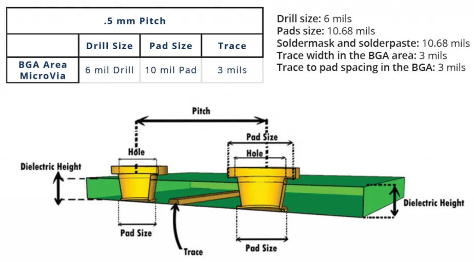
HDI Via-to-Via Spacing: What Happens When Vias Are Too Close?
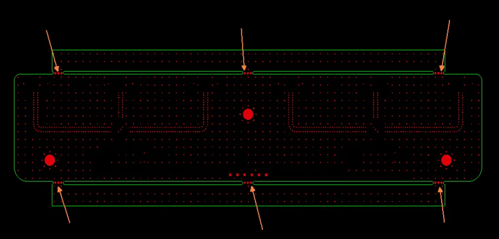
Why 0.267 mm Stamp-Hole Spacing Failed on Rogers RO4350B PTH Boards
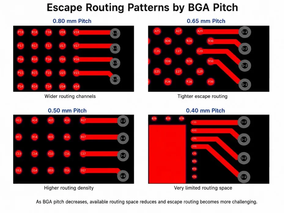
How HDI Connector Pin Density Affects HDI PCB Routing Decisions
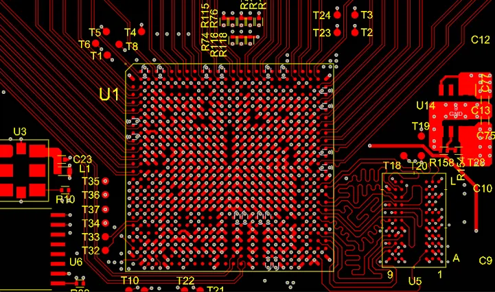
HDI PCB Via Keepout Zones: Where Should Components Be Avoided?
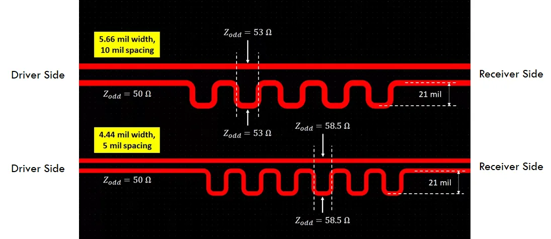
HDI Differential Pair Spacing: Common Layout Mistakes to Avoid
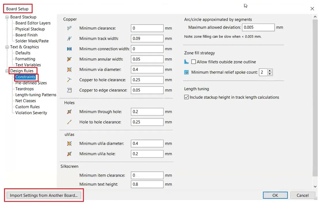
KiCad PCB Design Rules: How to Prepare Your Board for Manufacturing