


PCB Assembly
Printed circuit board (PCB) assembly represents a critical phase in electronics manufacturing, where components are mounted onto a board to create functional circuits. This process bridges design and production, ensuring that electronic devices perform reliably in diverse applications. From soldering techniques to component placement, PCB assembly encompasses the methods and technologies that transform bare boards into operational systems. Understanding these elements is essential for engineers, hobbyists, and industry professionals aiming to optimize production efficiency and product quality. Within this category, readers will find a comprehensive collection of guides that detail step-by-step assembly processes, tutorials on advanced tools like surface-mount technology and automated pick-and-place machines, and insights into troubleshooting common issues such as solder joint defects or thermal management challenges. Best practices are highlighted to promote reliability, including strategies for minimizing defects through quality control measures and adhering to industry standards like IPC guidelines. These resources draw from real-world expertise to address both fundamental concepts and cutting-edge innovations in the field. The practical value of mastering PCB assembly extends to numerous sectors, including consumer electronics, automotive systems, medical devices, and aerospace engineering. By applying the knowledge shared here, professionals can reduce manufacturing costs, accelerate time-to-market, and enhance device durability. For instance, effective assembly techniques ensure that circuits withstand environmental stresses, leading to longer-lasting products in demanding conditions. Delving into the articles in this PCB assembly category provides a pathway to deeper technical proficiency. Whether refining prototyping skills or scaling up production, the content equips readers with actionable strategies to tackle real-world challenges and stay ahead in an evolving industry.
Latest Blogs

What Manufacturing Teaches Design: Lessons from a Soldering Quality Problem
Analyze a QFN soldering defect caused by reduced pad spacing, connecting traces, and solder-mask compensation, with corrective PCB design guidelines and manufacturing feedback.

Key Manufacturing Technologies for Drone PCBs
Explore drone PCB manufacturing, including HDI, thick copper, high-Tg laminates, microvias, thermal management, and reliability testing for flight systems.

Compatible Pad Design and Soldering Reliability Validation for FCQFN and WLCSP Packages
Compare WLCSP and FCQFN compatibility using shared PCB pads and stencil designs, validated through X-ray, cross-section, thermal shock, and temperature-cycle testing.

Lead-Free Alloy Reflow Temperature Profiles and Analysis of Soldering Defects
Understand lead-free reflow temperature profiles, RSS and RTS methods, and how profiling controls wetting, solder voids, BGA head-in-pillow defects, and thermal limits.

Preventing Solder Paste Printing Defects in SMT: Practical Process Control from Stencil to SPI
Technical guide to preventing SMT solder paste printing defects through stencil management, print parameter tuning, alignment, solder paste control, SPI, and maintenance.
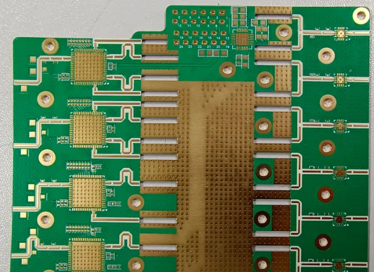
From Signal Frequency to Signal Integrity: What Is the Fundamental Difference Between High-Frequency and High-Speed PCBs?
Compare high-frequency and high-speed PCBs, covering frequency versus timing, Dk/Df materials, PTFE, signal integrity, applications, and design priorities.

Causes and Prevention of Solder Balls in Wave and Selective Soldering
Learn how solder balls form during wave and selective soldering, how flux and PCB solder-mask properties affect adhesion, and how process changes reduce defects.

DFM Deep Dive: Keep Vias Away from Pads to Prevent SMT Reflow Shorts and Tantalum Capacitor Offset
DFM guidance on via keep-out around SMT pads to prevent solder wicking and tantalum capacitor skew; covers 10 mil/12 mil limits and enforceable EDA checks.

The "Black Hole" on Pads: Why Via-in-Pad Must Be Filled or Avoided
DFM guidance for via-in-pad in PCB design: how resin fill prevents defects, when to use solder mask dams or move vias, plus a checklist for reliable joints.

DFM for D-PAK (TO-252): Prevent Solder Voids and Component Shift with Solder Mask Isolation and Segmented Pads
DFM guidance for D-PAK (TO-252): why solid copper ties cause solder voids and component shift, and how solder mask grids or segmented pads improve reflow and thermal reliability.
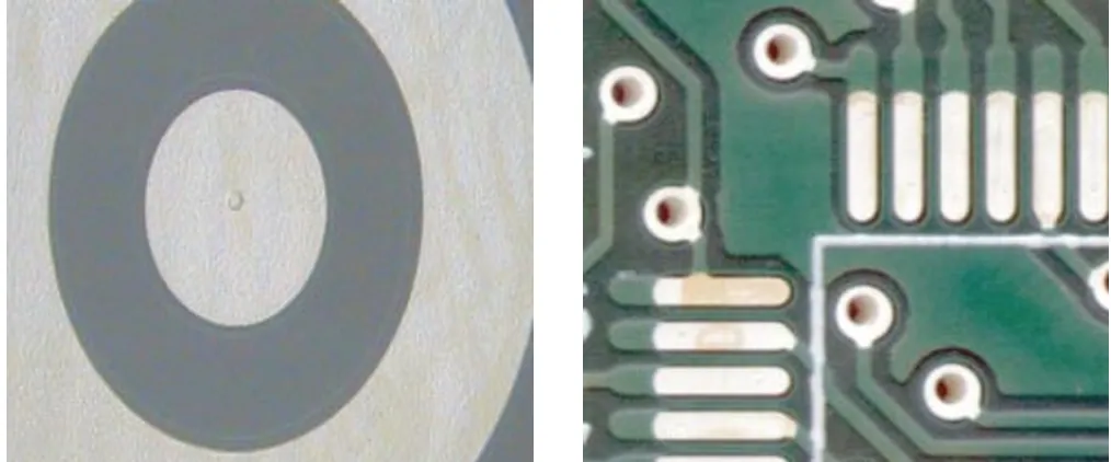
Immersion Silver (IAg) for PCBs: A Deep Dive into IPC-4553 and Practical Control Windows
Technical guide to IPC-4553 immersion silver: thickness control, solderability, acceptance criteria, handling/packaging rules, and self-limiting chemistry implications.

Solder Mask "Dams" Between SMT Pads: A Complete Guide to Solder Mask Coverage and NSMD Design
Practical rules for SMT pad-to-pad gaps: design solder mask dams and NSMD pads to prevent bridging and AOI false calls, with pitch exceptions and power-module guidance.


