










PCB Assembly
Printed circuit board (PCB) assembly represents a critical phase in electronics manufacturing, where components are mounted onto a board to create functional circuits. This process bridges design and production, ensuring that electronic devices perform reliably in diverse applications. From soldering techniques to component placement, PCB assembly encompasses the methods and technologies that transform bare boards into operational systems. Understanding these elements is essential for engineers, hobbyists, and industry professionals aiming to optimize production efficiency and product quality. Within this category, readers will find a comprehensive collection of guides that detail step-by-step assembly processes, tutorials on advanced tools like surface-mount technology and automated pick-and-place machines, and insights into troubleshooting common issues such as solder joint defects or thermal management challenges. Best practices are highlighted to promote reliability, including strategies for minimizing defects through quality control measures and adhering to industry standards like IPC guidelines. These resources draw from real-world expertise to address both fundamental concepts and cutting-edge innovations in the field. The practical value of mastering PCB assembly extends to numerous sectors, including consumer electronics, automotive systems, medical devices, and aerospace engineering. By applying the knowledge shared here, professionals can reduce manufacturing costs, accelerate time-to-market, and enhance device durability. For instance, effective assembly techniques ensure that circuits withstand environmental stresses, leading to longer-lasting products in demanding conditions. Delving into the articles in this PCB assembly category provides a pathway to deeper technical proficiency. Whether refining prototyping skills or scaling up production, the content equips readers with actionable strategies to tackle real-world challenges and stay ahead in an evolving industry.
Latest Blogs
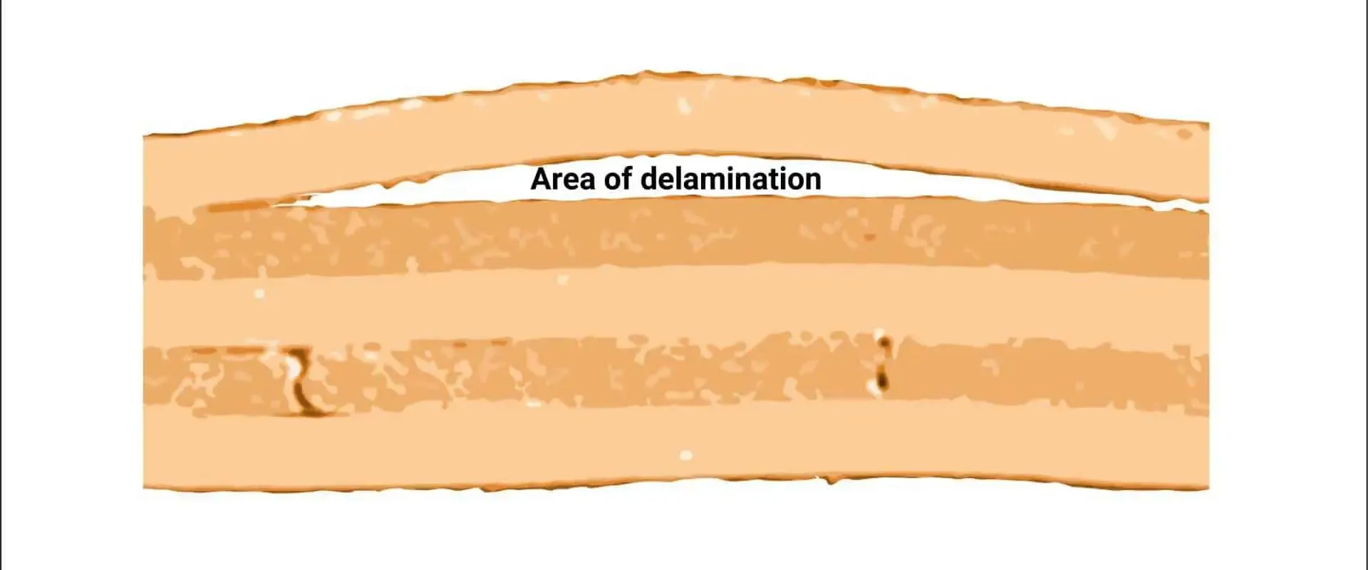
Preventing PCBA Delamination and PTH Cracking: Applying IPC-1602-2020 for Printed Board Handling and Storage
Engineering guide to IPC-1602-2020 on PCB handling and storage, focusing on moisture control, dry packaging, and ESD to prevent delamination during lead-free reflow.
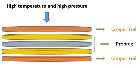
Decoding IPC-4101B: A Deep Dive into PCB Laminates and Prepregs
Technical guide to IPC-4101B: decoding PCB laminates and prepregs, key metrics (Tg, Td, Z-CTE), and QA processes including qualification, QCI, and SPC.

Deep Analysis: The BGA Rework Keep-Out Zone — Why You Must Not Place Components ≥ 3216 Directly Under a BGA
DFM guidance for BGA rework: enforce bottom-side keep-out (no components >3216 under BGAs) and same-side clearances (1, 2, 4 mm), plus latch spacing, case studies, checklist.

SMT Solder Joint Defect Case Study: Undersized Solder Balls on a CPU Socket
AXI flagged undersized solder balls on a CPU socket during SMT; teardown found solder wicking and a lot-specific material defect. Quarantine and new date code resolved.

DFM in Practice: The Hidden Tolerance Trap—Why SMT Connector Locating Pins Must Be Smaller Than the Hole
Explains why SMT connector plastic locating pins need a clearance fit in NPTH holes, detailing tolerance stack-up, reflow behavior, and a practical +0.3 mm hole-sizing rule.

Ionic Cleanliness Testing in SMT: Methods and Measurement Procedures
Guide to SMT ionic cleanliness testing with ROSE, ion chromatography (IC), and C3, detailing principles, procedures, strengths/limits, and method selection for quality control.
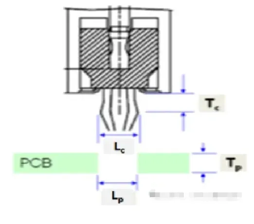
DFM in Practice: Zero-Pressure SMT Placement for Long DIMM Sockets — The Mechanics of Oval NPTH Holes and Locating Pins
DFM rule for zero-pressure placement of long DIMM sockets: prefer plastic locating posts; use oval NPTH holes for lock pins to improve seating and yield.

Wave Soldering Fixture Design Essentials for Process Engineers
Technical guide to wave soldering fixtures: materials, clearances, chamfers, thermal control, BGA reliefs, rail alignment, and spec-based PCB pallet design.

Manufacturing Process Study for 0.3 mm Pitch QFN Packages
Practical guide to manufacturing 0.3 mm pitch QFN: DFM-led PCB pad design, stencil optimization, micron placement, nitrogen reflow, and X-ray inspection.

ENIG "Black Pad" and BGA Solder Reliability: Failure Mechanism, Process Controls, and Acceptance Criteria
Technical guidance on PCB surface finishes: ENIG black pad mechanism, process controls, and SEM-based acceptance to reduce BGA solder failures.

Key Control Points for the Wave Soldering Process
Guide to wave soldering process control: equipment setup, flux spray and solder pot parameters, thermal profile, dwell time, pre-line checks, and maintenance.

Improving SMT Solder Joint Reliability Through Design and Process: From IMC Growth to HALT/HASA
Explains quality vs reliability, linking solder joint IMC kinetics to system HALT/HASA; covers reflow profiling, connector contacts, and polymer compatibility.


