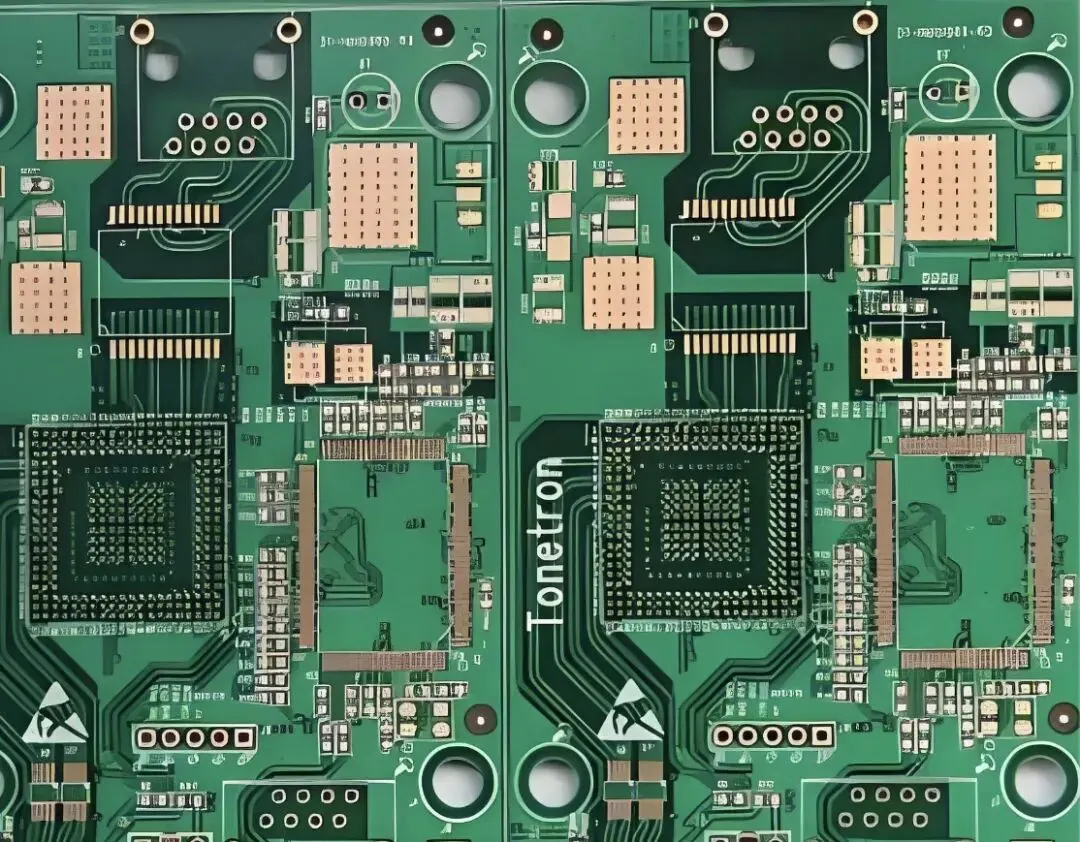
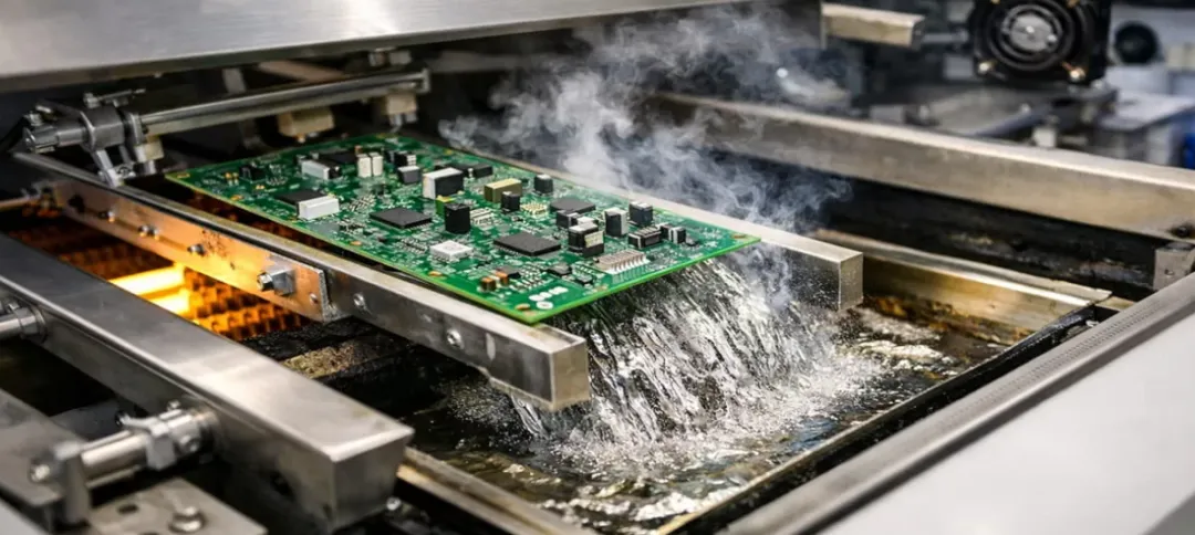
Delamination between the intermetallic compound (IMC) layer and the copper substrate after 500 hours of storage at 150 °C is a challenging packaging-reliability failure mode. It generally indicates that unfavorable changes have occurred at the interface or that excessive stress has accumulated during high-temperature exposure.
Several mechanisms can contribute to this type of delamination. In many cases, more than one factor is involved, with interfacial voiding, IMC growth, thermal stress, surface condition, solder composition, and initial joint quality interacting with one another.
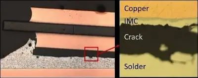
1. Excessive Formation and Coalescence of Kirkendall Voids
Mechanism
At elevated temperature, Cu atoms typically diffuse into the solder at a much higher rate than Sn atoms diffuse into Cu. The diffusion rates can differ by approximately one order of magnitude. This imbalance produces a net flux of atoms and leaves excess vacancies within the IMC layer or near the Cu/IMC interface, usually on the Cu side. The vacancies can accumulate and develop into Kirkendall voids.
These voids reduce the effective bonded area and weaken the mechanical strength of the interface. Once the interface has been weakened, thermal stress can more easily initiate cracks or cause separation between the copper and IMC layers.
Consequences of Long-Term Storage
As the high-temperature storage period increases, the number and size of the voids may increase. Individual voids can also connect along the interface, substantially reducing the bonding strength between Cu and the IMC. When the void density becomes sufficiently high, interfacial delamination can occur.
The 150 °C/500-hour storage condition provides both sufficient temperature and sufficient time to accelerate interdiffusion between Cu and Sn. Consequently, Kirkendall voiding can become highly pronounced and is often the most probable cause of Cu/IMC delamination under this type of condition.
2. Excessive IMC Growth and Phase Evolution
IMC Thickness and Brittleness
At high temperature, the diffusion reaction between Cu and the solder is accelerated, allowing the IMC layer to continue growing. IMCs are generally more brittle than the original Cu and solder materials. The initially formed η-Cu6Sn5 phase can continue to thicken, while an ε-Cu3Sn layer may form and grow beneath it.
As the total IMC thickness increases, internal stress can also increase. The greater brittleness of the IMC makes it more susceptible to cracking under stress or to separation from the Cu substrate. A thick IMC layer therefore does not necessarily indicate a stronger joint; beyond a certain condition, additional growth may degrade interfacial reliability.
Phase-Related Stress
Compared with η-Cu6Sn5, ε-Cu3Sn is generally more brittle. Its crystal structure and coefficient of thermal expansion differ from those of both the Cu substrate and the η-Cu6Sn5 layer. An excessively thick IMC layer, particularly one containing a substantial brittle Cu3Sn region, is therefore more vulnerable to cracking during thermal stress or subsequent cooling.
Phase evolution can also change the stress distribution through the interface. Long-term high-temperature exposure may cause IMC grain coarsening or morphological changes, such as a transition from a scallop-like structure to a more continuous layered structure. These changes can affect the mechanical interlocking and bonding strength between the IMC and the Cu substrate.
3. Thermal Stress Caused by CTE Mismatch
Cu, Cu6Sn5, Cu3Sn, and the solder have different coefficients of thermal expansion (CTEs). During heating, these materials expand at different rates. During cooling, they contract at different rates. The resulting mismatch generates thermal stress within the joint and at the interfaces between the different materials.
Repeated thermal expansion and contraction can produce cyclic stress. Over a long period, this stress may accumulate at locations where the structure is constrained or where the interface contains a geometric or material discontinuity. The resulting stress concentration can initiate or extend delamination.
Long-term exposure, such as 500 hours at high temperature, can contribute to interfacial fatigue. Thermal stress becomes particularly damaging when the interface has already been weakened by Kirkendall voids, brittle IMC, contamination, or poor initial wetting. In complex device structures or constrained assemblies, the local stress concentration may be even more severe.
4. Oxidation and Interfacial Contamination
Cu Surface Oxidation
Even slight oxidation of the Cu pad during manufacturing can reduce the quality of the subsequent bond. Oxidation may also occur if oxygen reaches the interface during high-temperature storage. The oxide layer can reduce solder wettability and weaken the chemical and mechanical bond between Cu and the IMC, making delamination more likely.
Contamination and Weak-Bond Regions
Before PCB soldering, the Cu surface may contain electroplating residues, fingerprints, oils, moisture, or other organic and inorganic contaminants. If these materials are not adequately removed by the flux and cleaning process, they can remain at the interface.
During high-temperature storage, trace organic materials or moisture may decompose, volatilize, or generate gas. Residues and gas pockets can create local stress concentrations or reduce adhesion at the Cu/solder interface. The result may be a weak-bond region that later develops into delamination.
Surface Finish and Roughness
The high-temperature stability of the selected Cu surface finish is also important. Finishes such as OSP, immersion silver, immersion tin, and ENIG can behave differently during prolonged thermal exposure. Depending on the material system and process conditions, a finish may degrade, dissolve, or react with the Cu and IMC layers, affecting interfacial strength.
Surface roughness can also influence the joint. A Cu surface that is excessively smooth may provide insufficient mechanical interlocking, while an excessively rough surface can interfere with uniform wetting and produce localized defects. The effect of roughness must therefore be evaluated together with the surface finish and soldering process.
5. Influence of Solder Alloy Composition
Lead-Free Solder
Common lead-free solders, such as SAC305, may be more susceptible than traditional SnPb solder to Kirkendall void formation and excessive IMC growth, particularly at elevated temperature. Alloying elements such as Ni, Co, and Bi can suppress IMC growth or modify IMC morphology. However, small deviations in alloy composition can also produce undesirable changes in interfacial behavior.
Impurity Elements
Trace impurities in the solder may segregate to the interface, alter the interfacial energy, or promote the formation of a particular IMC phase. These effects can change the microstructure and reduce the mechanical strength of the Cu/IMC interface. For this reason, solder composition and material consistency should be considered when the failure is not explained by voiding or process defects alone.
6. Process Defects and Initial Joint Quality
Reflow Profile and Initial IMC Condition
An inappropriate reflow process, including insufficient temperature, inadequate time above liquidus, excessive peak temperature, or an unsuitable cooling rate, can produce an initial IMC layer that is too thick or nonuniform. Small defects may also be present at the interface, including microvoids and areas of incomplete wetting.
These initial defects can act as origins for delamination during subsequent high-temperature storage. A defect that is not immediately large enough to cause failure may expand when exposed to continued interdiffusion and thermal stress.
Insufficient Initial Bond Strength
Deficiencies in the original joining process can reduce the initial strength of the IMC/Cu interface. Examples include poor solder wetting, insufficient bonding pressure, and inadequate surface cleanliness. During long-term high-temperature exposure, these weaknesses may be amplified until they become visible as interfacial delamination.
Residual Stress
Manufacturing can also introduce residual stress through curing shrinkage, nonuniform cooling, or other process-related effects. When this residual stress combines with thermal stress during storage, the total stress at the interface may exceed the local bonding strength and promote separation.
7. Moisture and Vapor Pressure
If the product absorbs moisture before high-temperature storage, the moisture may vaporize during heating and generate vapor pressure. When small defects or pores are present at the interface, this pressure can act on the surrounding material and accelerate delamination.
Moisture-related separation is often more apparent during reflow, but long-term high-temperature storage can also aggravate defects that already exist. Moisture should therefore be considered when the failure is associated with pores, weak-bond regions, or evidence of volatile residues.
Failure Analysis and Root-Cause Identification
Determining the exact cause requires observation of the delamination morphology, the location of the separation, and the composition of the adjacent materials. The following analytical methods are useful.
- Cross-sectioning: Prepare cross-sections through the delaminated regions to determine the IMC thickness, void distribution, and precise separation location. The delamination may occur within the IMC, at the IMC/Cu interface, or at another interface in the joint.
- Scanning electron microscopy and energy-dispersive X-ray spectroscopy: SEM can reveal the microscopic morphology of the fracture or delamination surface, while EDS can identify the elemental composition and help determine whether oxidation, contamination, or abnormal elements are present.
- X-ray photoelectron spectroscopy: When surface oxidation or contamination is suspected, XPS can provide more detailed information about the chemical state and composition of the surface.
Careful correlation between the delamination location, IMC morphology, void distribution, and elemental composition is necessary to distinguish the primary cause from secondary aggravating factors.
Conclusion
For Cu/IMC delamination observed after 500 hours of storage at 150 °C, excessive formation and coalescence of Kirkendall voids is one of the most probable causes. Excessive IMC growth, particularly growth of the brittle Cu3Sn layer, can also contribute significantly. Thermal stress caused by CTE mismatch, Cu surface contamination or an unsuitable surface finish, solder alloy composition, and poor initial joint quality may act as additional causes or aggravating factors.
The first step in resolving the problem is a detailed cross-sectional SEM/EDS investigation. Particular attention should be paid to the region near the delamination interface, especially on the Cu side, to determine whether a high density of fine voids is present. The analysis should also measure IMC thickness and document its morphology. These observations provide direct evidence for identifying the root cause and selecting an effective corrective action.
In comparable failure analyses, numerous fine voids concentrated near the Cu/IMC interface are a strong indication that the Kirkendall effect is contributing to delamination. Once the void distribution, IMC structure, surface chemistry, and initial process condition have been correlated, the appropriate improvement direction can usually be defined more clearly.