After completing a hardware design, selecting the components, laying out the PCB, and sending the Gerber files to the board manufacturer, the manufacturing process still has an important question to answer: why do some components go through reflow soldering while others are processed by wave soldering? Both processes melt solder and attach components to the PCB, so why does a production line need two different types of equipment?

The reason is not simply that equipment manufacturers have made the process unnecessarily complicated. The fundamental difference between reflow soldering and wave soldering lies in how solder reaches the joint and which component structures each process can handle effectively.
For hardware engineers, understanding these two processes is not merely a matter of manufacturing knowledge. The choice of soldering process can affect PCB layout, component-package selection, pad design, assembly yield, and subsequent failure analysis.
Reflow Soldering: Apply Solder Paste, Then Heat the Assembly
Reflow soldering is primarily used for SMT components, including resistors, capacitors, SOP packages, QFN packages, and BGAs.

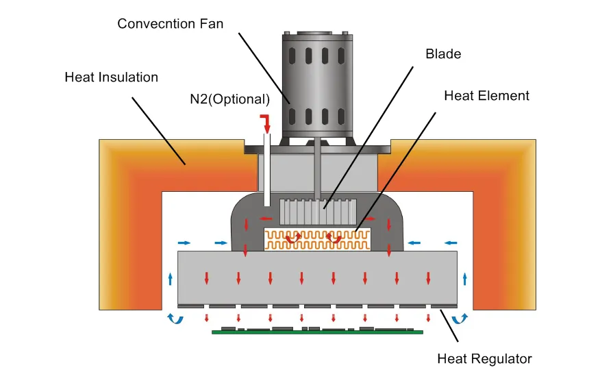
The basic process is to print solder paste onto the PCB pads, place the components, and then pass the entire assembly through a reflow oven. The solder paste goes through preheating, temperature ramp-up, time above the liquidus temperature, and cooling. These stages allow the solder to melt, wet the component terminations and PCB pads, and then solidify into joints.
A commonly overlooked detail is that reflow soldering does not simply heat the entire PCB to one fixed temperature and stop. The temperature must be controlled as a function of time. The reflow profile determines how quickly the board heats, how long it remains at different temperature ranges, how long the solder stays above its liquidus temperature, and how quickly the assembly cools.

For SAC305 lead-free solder, the melting point is approximately 217 °C. In an actual reflow profile, the joint temperature normally rises above the liquidus temperature and remains there for a controlled period. The exact peak temperature, time above liquidus, and heating and cooling rates depend on the solder paste, the temperature rating of the components, and the thermal mass of the PCB. These parameters should not be treated as universal fixed values.
Why Must the Reflow Profile Be Controlled So Carefully?
Consider a PCB that contains small-package resistors, large connectors, and power pads connected to extensive copper areas. Small components have relatively low thermal mass and heat up quickly. Large pads and components absorb more heat and therefore heat up more slowly.
If the temperature rises too quickly, the small components may approach their peak temperature while the solder on the large pads has not yet melted sufficiently. Conversely, if the peak temperature or the time at high temperature is extended to accommodate the large pads, the assembly may experience greater component thermal stress, PCB damage, or solder oxidation.

The real challenge of reflow soldering is therefore to deliver enough heat to every solder joint, but not more heat than the components and PCB can safely tolerate. Differences in copper area, component size, pad geometry, and board thickness can all affect the thermal balance across the assembly.
Wave Soldering: Direct Contact with Molten Solder
Wave soldering uses a more direct mechanism. The equipment melts the solder and uses a pump to generate a stable wave of molten solder. After the PCB passes through flux application and preheating, the soldering side of the board contacts the solder wave. The molten solder wets the component leads and PCB pads, forming the joints.

The classic application for wave soldering is the through-hole component, also called a THT component. Examples include through-hole connectors, transformers, relay sockets, and some high-power components. Their leads pass through the PCB holes, and the solder wave reaches the leads and pads on the solder side of the board. Proper wetting then forms the electrical and mechanical connection.

Why Not Process Every PCB with Wave Soldering?
Wave soldering causes molten solder to contact a local region of the PCB directly. If a board contains a large number of SMT components, especially fine-pitch leads or bottom-terminated packages, the solder can bridge adjacent leads. Components that are not suitable for direct contact with the solder wave may also experience excessive heating or incomplete soldering.

Wave soldering also requires careful consideration of the PCB travel direction, pad spacing, solder-mask design, lead extension, and component placement on the solder side. If the board layout is not designed for the process, stable mass production can be difficult even when the equipment parameters are properly adjusted.
It is important to avoid an overly rigid classification in which reflow soldering is considered suitable only for SMT components and wave soldering only for through-hole components. Actual production may also use selective wave soldering and through-hole reflow soldering. The appropriate method depends on the package structure, component distribution, required joint reliability, and production-capacity requirements.

Design Details Hardware Engineers Should Understand
Hardware engineers do not necessarily need to operate soldering equipment themselves, but they should understand how design decisions affect assembly.
- Package and pad design must support the soldering process. Electrical connectivity is only one design consideration. QFN and BGA packages place specific demands on solder-paste printing, pad geometry, and the reflow profile. Through-hole pads must be designed with the hole diameter, copper thickness, lead dimensions, and solder filling requirements in mind.
- Large copper areas change the thermal distribution. When a power-component pad is connected to a large copper pour, heat can be conducted away from the joint. This may cause insufficient local heating during reflow. Thermal mass, pad structure, and the actual measured temperature profile should be considered together. Simply increasing the oven temperature is not always an appropriate solution.
- Assembly defects are not necessarily component-quality problems. For example, a resistor that stands on end after reflow may be affected by uneven heating at its two pads, unequal solder-paste volume, or placement offset. A connector that develops solder bridges after wave soldering may be affected by pad spacing, lead orientation, flux conditions, or wave parameters.

The Key Difference Between the Two Processes
Reflow soldering controls the thermal profile of solder paste as the entire PCB assembly passes through the oven. Wave soldering controls the contact between molten solder and the soldering surface of the PCB. One process is primarily based on controlled heating of the complete assembly, while the other relies on direct contact with a moving solder wave.
Neither process is inherently more advanced than the other. Each is suited to different component packages, PCB structures, layout conditions, and production requirements. A robust design therefore considers the assembly process from the beginning rather than treating soldering as a manufacturing detail to be addressed after the PCB has been completed.