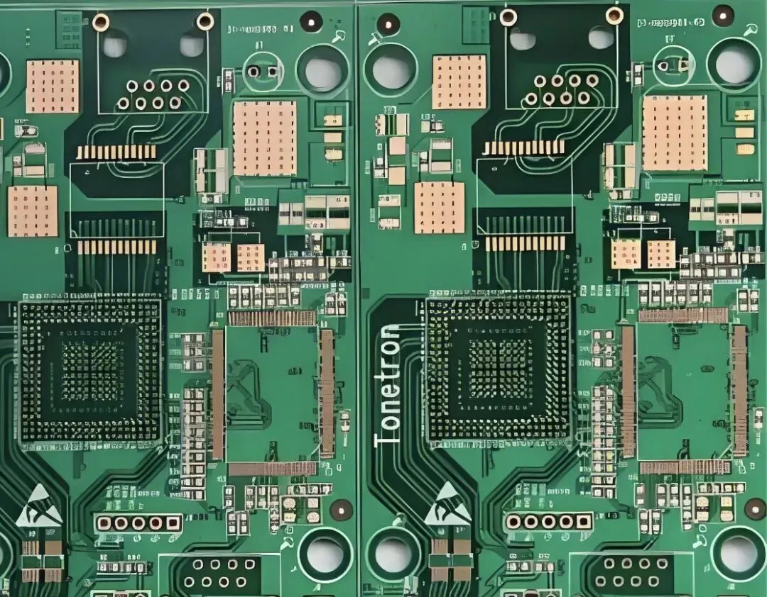
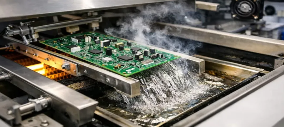
Solder beads are a common defect in reflow soldering. They typically appear along both sides of leadless chip components such as resistors and capacitors. These beads vary in size, are isolated, and are not connected to adjacent solder joints. While they degrade product appearance, the more serious concern is electrical reliability: stray solder beads can dislodge and cause intermittent shorts, reduce insulation resistance in contaminated areas, or introduce latent reliability risks after environmental stress.
In practice, solder beads can result from multiple sources: solder paste selection and handling, stencil design, printing setup and alignment, placement pressure, reflow temperature profile, and residual contamination during rework. Addressing the issue requires a holistic look at the solder paste printing and reflow process. The sections below explain typical root causes and offer practical remedies.
1. Inappropriate Stencil Apertures
Excess paste volume and improper aperture shapes are among the most frequent drivers of solder bead formation. Oversized stencil apertures or shapes that do not confine paste to the pad can allow solder paste to spread beyond the pad (especially on chip components). During placement, the component body compresses the paste; the squeezed-out paste can separate and, during reflow, coalesce into isolated solder beads adjacent to the component.
Recommended practices:
- Aperture size. For chip-size resistors and capacitors, set the stencil aperture slightly smaller than the PCB pad to compensate for etching tolerances and prevent paste over-deposition. A practical guideline is to size the aperture at approximately 90–95% of the corresponding PCB pad area.
- Aperture shape. Choose aperture geometries that control paste volume and limit squeeze-out. For chip components, options such as tapered "home-plate," modified rectangles, or windowed designs can reduce paste mass near the component centerline and direct wetting toward the pad edges. This helps achieve proper fillet formation while minimizing paste extrusion under the component body.

Complementary considerations include selecting an appropriate stencil thickness for the component mix, ensuring good gasket contact between stencil and board, and maintaining adequate solder mask dams between adjacent pads so that displaced paste is physically contained. Excess placement pressure can also exacerbate paste squeeze-out; reducing placement force to the minimum needed for accurate seating helps prevent bead formation.
2. Misregistration During Solder Paste Printing
Stencil-to-board misalignment is another major cause of solder beads. If the stencil and PCB are not registered accurately or if either is inadequately secured, paste can smear or bridge onto solder mask areas. This misplaced paste becomes a source of isolated solder particles during reflow.
Recommended practices:
- Ensure precise alignment. Use board fiducials and a stable clamping/locating system so that the stencil and PCB remain aligned throughout the print cycle.
- Optimize printing parameters. Whether printing is manual, semi-automatic, or fully automatic, operators must set and verify squeegee pressure, speed, and separation (snap-off). Overpressure or excessive speed can force paste under the stencil or beyond pad boundaries. Proper release depends on the paste's rheology, aperture area ratio, and the separation profile.
- Maintain stencil and process cleanliness. Regularly clean the stencil underside to prevent paste accumulation and smearing. Implement a controlled cleaning interval based on inspection feedback and paste behavior.
Solder paste printing is the first and one of the most critical steps in surface-mount assembly. Defects originating at the printing stage often dominate overall assembly defect rates, so disciplined setup, verification, and inspection of the printing process are essential.
3. Improper Handling of Solder Paste
Moisture uptake and improper conditioning of solder paste can lead to solder beads. If refrigerated paste is not allowed to equilibrate to room temperature before opening, condensation and uneven viscosity may result. Moisture and volatile solvents entrained in the paste can rapidly vaporize during reflow, causing spattering and propelling small paste particles off the pads, which then reflow into beads.
Recommended practices:
- Warm-up before use. Bring refrigerated paste to room temperature before opening the container to prevent condensation and achieve stable rheology. A common practice is to allow approximately 4 hours of equilibration, then mix thoroughly for a uniform consistency.
- Avoid moisture uptake. Keep containers sealed when not in use and minimize exposure to ambient humidity. Do not add thinners or solvents that can change volatility or metal loading unless explicitly supported by the paste supplier.
- Respect shelf life and working time. Use paste within its specified shelf life and on-line open time. Paste beyond its working window may slump or exhibit increased spattering.
4. Incorrect Reflow Temperature Profile
An ill-suited reflow profile is a frequent cause of solder bead formation. If the preheat and soak phases are too short or at inadequate temperatures, solvents in the paste may not outgas sufficiently before the reflow zone. A rapid temperature rise then drives violent outgassing, which can propel micro-droplets of solder and flux off the pads. These droplets later solidify as beads.
Recommended practices:
- Use a full-profile approach. A standard reflow profile includes preheat, soak, reflow, and cooling. The preheat and soak stages minimize thermal shock to components and the PCB while allowing paste volatiles to escape in a controlled manner.
- Soak parameters. As a reference point, a soak range of approximately 150–160 °C for 70–90 s helps promote solvent evaporation without prematurely activating or depleting flux. Actual values must be tuned to the specific paste, oven, board thermal mass, and component mix.
- Control heat ramp rates. Excessively steep ramps can drive spattering. Use measured thermocouple profiles on representative boards to validate that each zone meets the intended temperature and dwell targets.
- Verify consistency. Adjust and verify the profile before each production run or after significant changes in board design, panelization, or component population.
5. Residual Solder Paste Left on Boards
During process setup—especially when adjusting or debugging the stencil—some boards may require paste reprinting. If the previously deposited paste is not fully removed, the residual paste can migrate during reflow and form beads, or it can cause more serious defects such as solder bridges or plugged through-holes.
Recommended practices:
- Fully remove prior deposits. Carefully scrape excess paste from the PCB, taking care not to push paste into plated through-holes or vias.
- Clean with compatible solvents. After gross removal, clean the board with a suitable solvent to remove residual paste and flux. If residues are difficult to remove, use an ultrasonic cleaner with a compatible solvent for around 1 minute to effectively dislodge trapped paste.
- Dry thoroughly. Ensure boards are dry before reprinting to avoid moisture entrapment.
Removing Solder Beads from Assembled Boards
Once solder beads are present on an assembled PCB, flux residues can help them adhere to the surface, making manual removal time-consuming or impractical. In such cases, cleaning with a solder paste-compatible cleaning agent is effective. Ultrasonic cleaning often yields better results by mechanically dislodging small beads without damaging solder joints when used with appropriate settings and solvents.
When selecting a cleaning process, verify compatibility with components, markings, and conformal coatings, and evaluate ionic contamination levels after cleaning if the product requires high reliability. Consistent process control and post-clean inspection help confirm that beads are fully removed and that no new residues are introduced.
Summary
Solder beads are a multi-factor defect driven by paste volume control, printing alignment and parameters, paste conditioning, reflow profiling, and cleanliness during rework. Effective mitigation starts with stencil design—limiting aperture size to around 90–95% of pad area for chip components and selecting aperture shapes that reduce central paste volume. Robust printing alignment and parameter control, proper paste handling, and a well-tuned reflow profile with adequate preheat/soak are equally critical. Finally, disciplined removal of residual paste during process adjustments and appropriate cleaning methods for assembled boards ensure beads do not persist. Addressing these factors as a system significantly reduces bead occurrence, enhances solder joint quality, and improves long-term reliability.