










PCB Component Installation in SMT Assembly
What This Video Covers
This video details the critical component installation stage of PCB manufacturing, focusing on surface-mount technology (SMT) placement, through-hole insertion, soldering methods, and post-assembly inspection. It explains how automated pick-and-place systems achieve micron-level accuracy, followed by reflow soldering and rigorous electrical testing to guarantee long-term reliability.
The content highlights key engineering considerations such as component orientation, thermal profiles, and mechanical stress management during installation. These processes are essential for producing high-density interconnect (HDI) and multilayer PCBs that meet stringent performance requirements.
OEM engineers and procurement teams working on aerospace, automotive electronics, medical devices, and industrial control systems will find the information directly applicable. For project pricing, request an instant PCB assembly quote or explore full PCB assembly services.
Key Highlights
- Precision SMT placement and reflow soldering ensure accurate component installation on multilayer and HDI PCBs while maintaining signal integrity and thermal performance.
- Automated processes combined with thorough inspection deliver high-yield, reliable assemblies suitable for mission-critical applications in aerospace, automotive, and medical electronics.
- Proper component installation techniques minimize mechanical stress and support the demanding reliability standards of industrial control and IoT devices.
Precision SMT Placement and Automated Pick-and-Place Systems
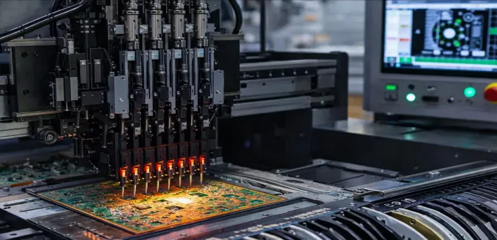
The automated pick-and-place machine forms the backbone of modern PCB component installation, positioning thousands of surface-mount devices per hour with positional accuracy often below 25 microns. Vision systems and fiducial markers enable real-time alignment corrections, compensating for minor board warpage or material expansion.
In high-volume production, nozzle selection, feeder setup, and component library calibration directly influence placement yield. Improper vacuum pressure or nozzle wear can lead to dropped components or rotated parts, resulting in rework or scrap. Manufacturers apply DFM principles by standardizing component orientations and maintaining adequate spacing to facilitate reliable pickup and placement.
For dense HDI designs, sequential placement strategies and localized heating prevent thermal gradients that cause board flexing. Real-world production data shows that optimized placement parameters reduce defect rates by up to 40% in complex multilayer boards used in automotive and medical applications.
Reflow Soldering and Thermal Profile Optimization
Reflow soldering follows component placement and demands carefully engineered thermal profiles to form reliable intermetallic bonds without damaging sensitive parts. A typical profile includes preheat, soak, reflow peak, and cooling stages, with peak temperatures tailored to solder paste alloy specifications (commonly SAC305).
Deviations in ramp rates or insufficient soak time frequently cause defects such as voiding, head-in-pillow, or component floating. Production teams monitor profiles using thermocouples placed at multiple board locations, especially near large thermal mass components like BGAs or connectors.
Practical recommendations include balancing airflow in convection ovens and using nitrogen atmospheres for high-reliability assemblies to minimize oxidation. In rigid-flex and HDI boards, careful attention to zonal heating prevents delamination or warpage during the reflow phase.
Common Manufacturing Challenges in PCB Component Installation
Component misalignment remains one of the most frequent issues in PCB component installation, often stemming from inaccurate fiducial recognition, vibration in the placement head, or inconsistent board panelization. These defects lead to open circuits, shorts, or compromised signal integrity, particularly in high-speed designs.
Tombstoning and skewing of small passive components arise from uneven solder paste deposition or asymmetric thermal gradients. Mitigation involves balanced pad designs, uniform stencil apertures, and verified paste volume through solder paste inspection (SPI) systems prior to placement.
Mechanical stress during installation can crack ceramic capacitors or delaminate pads, especially on thin or flexible substrates. Manufacturers address this through controlled placement force, appropriate support tooling, and selection of components rated for the intended assembly process. Thorough root-cause analysis using cross-sectioning and X-ray inspection helps refine processes for consistent high-yield outcomes.
Aspect Comparison
| Aspect | SMT Installation | Through-Hole Installation | Mixed Technology Impact |
|---|---|---|---|
| Placement Accuracy | <25 microns typical | Manual or wave selective | Requires sequential process planning |
| Thermal Considerations | Critical reflow profile control | Wave or selective soldering | Risk of multiple thermal cycles |
| Defect Commonality | Tombstoning, misalignment | Insufficient fill, barrel cracks | Increased inspection complexity |
| Typical Applications | High-density HDI, consumer/medical | Connectors, high-power components | Aerospace and automotive boards |
Design for Manufacturability Guidelines for Reliable Component Placement
Effective DFM for PCB component installation begins at the layout stage with standardized footprints, adequate clearance around fine-pitch devices, and consideration of assembly panelization. Component orientation should minimize rotation during placement and align with tape-and-reel or tray feeding directions to reduce setup time and errors.
Designers benefit from consulting manufacturer capabilities early, verifying minimum component-to-component spacing, and incorporating self-centering pad geometries for small passives. For HDI and rigid-flex constructions, thermal relief patterns and via placement must balance electrical performance with soldering heat distribution.
Practical production experience demonstrates that boards designed with assembly in mind achieve first-pass yields exceeding 98%, significantly reducing costs and lead times for mission-critical projects. Collaboration between design and manufacturing teams on component selection, polarity marking, and test point accessibility further enhances overall reliability.
Post-Installation Inspection and Quality Assurance Protocols
Post-installation verification combines 3D AOI for visible joint quality, X-ray for hidden connections under BGAs and QFNs, and electrical testing. These layered inspections catch defects that visual checks alone would miss, such as head-in-pillow or voiding in solder joints.
Statistical data from inspection systems feeds back into process adjustments, enabling continuous improvement in placement accuracy and reflow consistency. For critical applications, additional burn-in or environmental stress screening validates long-term performance under operating conditions.
Effective quality control integrates these methods into a closed-loop system that correlates defects with upstream parameters, reducing scrap and enhancing overall manufacturing efficiency.
FAQ
Q1: How does component placement accuracy affect the performance of HDI and multilayer PCBs?
A1: High placement accuracy prevents misalignment that can cause short circuits, open connections, or impedance mismatches, directly improving signal integrity and long-term reliability in dense board designs.
Q2: What quality checks are performed after SMT component installation during PCB assembly?
A2: Post-installation inspection includes automated optical inspection (AOI), X-ray analysis, in-circuit testing (ICT), and functional testing to verify correct component placement, solder joints, and overall board performance.
Q3: Which industries require the most rigorous component installation standards for PCB assemblies?
A3: Aerospace, automotive electronics, medical devices, and industrial control systems demand the highest standards due to strict reliability, vibration resistance, and thermal management requirements.
Q4: What are the primary causes of tombstoning during PCB component installation and how can it be prevented?
A4: Tombstoning typically results from uneven solder paste volume, asymmetric heating, or imbalanced pad designs. Prevention involves symmetric pad layouts, precise stencil printing verified by SPI, optimized reflow profiles, and selection of components with appropriate termination styles.
Q5: How should designers prepare footprints for mixed SMT and through-hole component installation?
A5: Footprints must accommodate sequential processing, provide adequate clearance for soldering tools or wave pallets, and include proper thermal reliefs. DFM reviews should confirm compatibility with automated placement equipment and inspection access for both technologies.
Welcome to AIVON PCB. Today, we're showing you a clean and precise SMD component installation.
First, we prepare the PCB board and carefully align the surface-mount components onto the pads.
Next, we apply flux to ensure perfect solder flow and heat distribution.
Using controlled heat from the hot air station (or soldering iron), we reflow the solder... Watch how the components settle perfectly into place.
And that's it — clean joints, no bridges, no damage. Professional results every time.
What problem should we fix next? Let us know in the comments!
Follow AIVON for more soldering tips, PCB repairs, and electronics know-how.





