










SMD Stencil Explained: How Precise Solder Paste Printing Works on PCBs
Key Moment
What This Video Covers
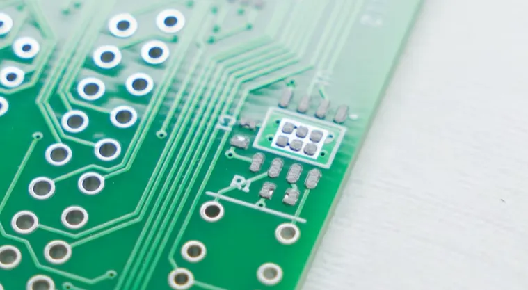
This video explains how SMD stencils achieve precise solder paste printing on PCB pads during SMT assembly. An SMD stencil is a thin stainless-steel sheet with laser-cut apertures that deposit solder paste only where components must be placed.
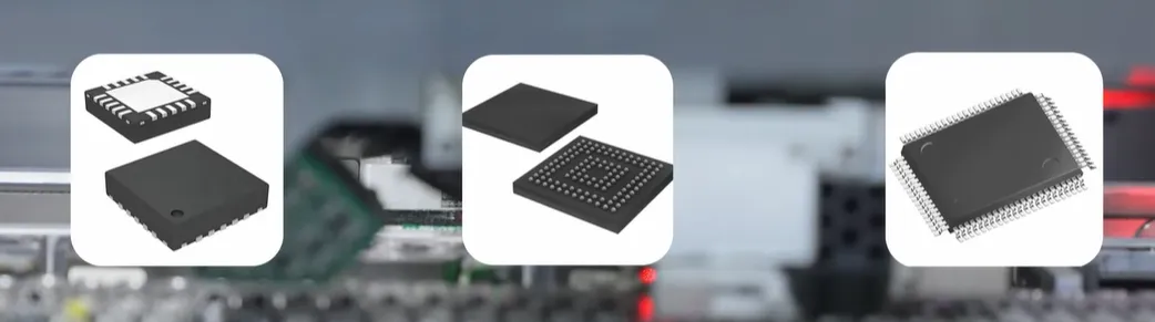
The stencil controls paste volume through precise thickness (0.08-0.13 mm), aperture design, surface smoothness, and release performance. These factors are critical for fine-pitch devices such as QFNs, BGAs, and small ICs, where excess paste causes bridging and insufficient paste leads to weak joints. Optional electropolishing or nano-coating further improves paste release and reduces defects.
The video covers stencil use from prototyping through small-batch production, ensuring consistent results and reliable solder joints from the first build. It also highlights our manufacturing capabilities in custom laser-cut stencils available in both framed and frameless formats.
For project support, review our SMT stencil specifications or request an SMT stencil quote. Full assembly support is available through our PCB assembly quote page.
Key Highlights
- Laser-cut apertures in stainless-steel SMD stencils deliver precise solder paste volume exactly on PCB pads for consistent SMT results.
- Stencil thickness, aperture design, and optional electropolishing or nano-coating optimize paste release and minimize defects on fine-pitch components.
- Suitable for prototyping to small production runs, supporting reliable assembly of QFNs, BGAs, and other high-density devices.
Laser-Cut Apertures and Paste Volume Control
Laser cutting produces apertures with near-vertical walls and tight dimensional tolerance, typically within ±0.01 mm. The resulting aperture size and shape define the theoretical paste volume deposited on each pad. For area-array devices the aperture is often reduced relative to the pad (for example 80–90 % of pad area) to limit excess paste that would otherwise squeeze out and form bridges.
Aperture design must also satisfy the area-ratio rule of thumb used in SMT process engineering: the ratio of aperture opening area to wall area should remain above approximately 0.66 for reliable paste release. When the ratio falls below this value, paste tends to stick to the aperture walls, producing insufficient solder on the pad. Laser-cut stainless-steel stencils maintain the geometric accuracy needed to keep area ratios within acceptable limits even for 0.4 mm and 0.5 mm pitch devices.
Surface roughness left by the laser can still impede release. Subsequent electropolishing or nano-coating removes microscopic peaks and creates a smoother wall, further improving transfer efficiency. In production environments these refinements reduce the frequency of incomplete prints that would otherwise require stencil cleaning or board rework.
Stencil Thickness Guidelines for Fine-Pitch Devices
Stencil thickness is the primary lever for controlling absolute paste volume. Standard production thicknesses range from 0.08 mm to 0.13 mm. Thinner foils (0.08–0.10 mm) are preferred for fine-pitch QFNs, BGAs, and 0201 or smaller passive packages because they limit the volume of paste that can be deposited and thereby reduce the risk of bridging. Thicker foils (0.12–0.13 mm) are used when larger components or higher stand-off heights require greater solder volume.
Selecting an incorrect thickness creates predictable failure modes. A 0.13 mm stencil applied to 0.4 mm pitch QFN pads frequently deposits enough paste to form bridges between adjacent pins after reflow. Conversely, a 0.08 mm stencil used on large power pads or connectors can leave insufficient solder, resulting in weak mechanical joints or open electrical connections. Process engineers therefore match thickness to the finest pitch present on the board while verifying that coarser features still receive adequate volume, often by adjusting individual aperture sizes rather than changing the entire foil thickness.
The table below summarizes common thickness recommendations based on component pitch and typical application.
| Component Pitch / Type | Recommended Stencil Thickness | Primary Risk if Too Thick | Primary Risk if Too Thin |
|---|---|---|---|
| ≤ 0.4 mm (fine-pitch QFN/BGA) | 0.08–0.10 mm | Bridging | Insufficient solder |
| 0.5–0.65 mm | 0.10–0.12 mm | Bridging on dense areas | Weak joints on large pads |
| ≥ 0.8 mm or mixed large pads | 0.12–0.13 mm | Excess paste on fine areas | Open joints |
| Prototype / mixed technology | 0.10–0.12 mm (step stencil) | Local volume mismatch | Local volume mismatch |
Electropolishing and Nano-Coating Effects on Paste Release
After laser cutting, aperture walls retain microscopic striations. Electropolishing removes a thin surface layer, rounding peaks and producing a smoother finish that reduces adhesion of solder paste. Nano-coating applies a thin hydrophobic or oleophobic film that further lowers surface energy, allowing paste to release cleanly with less residual material left inside the aperture.
In real production runs these treatments lower the incidence of two common defects: insufficient solder (caused by paste remaining in the aperture) and mid-chip solder balls (caused by paste that is partially released and then redeposited irregularly). Boards assembled with untreated stencils often require more frequent underside cleaning and higher under-stencil wipe rates, increasing cycle time and consumable use. Treated stencils maintain stable transfer efficiency over longer print runs, which is especially valuable when printing high-mix prototype panels or small production lots where process window margin is limited.
Framed Versus Frameless Stencil Selection by Production Volume
Frameless stencils consist of the stainless-steel foil alone and are typically held in a reusable tensioning frame at the printer. They offer lower unit cost and shorter lead times, making them suitable for prototype and low-volume builds where frequent design changes occur. Framed stencils are permanently bonded into an aluminum or stainless-steel frame that maintains consistent tension and alignment; they provide greater dimensional stability and are preferred for higher-volume or automated lines that demand repeatable registration over many prints.
Choosing the wrong format introduces practical issues. A frameless stencil used on a high-speed printer without adequate tensioning can exhibit local foil movement, producing mis-registration and incomplete paste transfer. A framed stencil ordered for a one-time prototype adds unnecessary cost and storage volume. Matching the stencil format to expected build quantity and printer capability therefore forms part of standard DFM review before the first print.
Common Solder Paste Printing Defects and DFM Prevention
Insufficient solder, bridging, and solder-ball formation remain the most frequent defects linked to stencil performance. Insufficient solder occurs when paste fails to release fully from the aperture, often because of low area ratio, rough walls, or excessive stencil thickness relative to pitch. Bridging results from over-volume deposition or aperture designs that allow paste to spread beyond pad edges. Solder balls can form when paste is partially released and then displaced during component placement or reflow.
Prevention centers on three controllable factors: maintaining area ratio above 0.66, selecting thickness matched to the finest pitch, and specifying electropolishing or nano-coating when fine-pitch devices dominate the bill of materials. In addition, aperture wall taper (slightly larger opening on the PCB side) and proper printer parameters (snap-off, squeegee pressure, and speed) further stabilize the process. When these DFM rules are observed, first-pass print yields improve and the need for post-print inspection or rework declines.
FAQ
Q1: What stencil thickness is recommended for fine-pitch QFN and BGA components?
A1: Thicknesses between 0.08 mm and 0.10 mm are typically chosen for fine-pitch devices to control solder volume and prevent bridging.
Q2: How do electropolishing and nano-coating improve SMD stencil performance?
A2: Both treatments create smoother aperture walls, enhancing solder paste release and significantly reducing defects such as insufficient solder or bridging.
Q3: Should I order a framed or frameless SMD stencil for prototype builds?
A3: Frameless stencils are cost-effective and flexible for prototypes and low-volume runs, while framed stencils provide better stability for higher-volume or automated production.
Q4: What area ratio should be maintained for reliable solder paste release from an SMD stencil?
A4: An area ratio (aperture opening area divided by wall area) of at least 0.66 is the widely accepted minimum for consistent paste transfer. Ratios below this value increase the likelihood that paste will remain inside the aperture, resulting in insufficient solder on the pad.
Q5: How does incorrect stencil thickness cause bridging or open joints in SMT assembly?
A5: Excess thickness deposits too much paste on fine-pitch pads, allowing solder to bridge adjacent pins after reflow. Insufficient thickness leaves too little paste on larger pads or connectors, producing weak mechanical joints or open electrical connections. Matching thickness to the finest pitch while adjusting individual apertures for coarser features avoids both extremes.
How does solder paste get printed so precisely onto tiny pads on a PCB?
That's what an SMD stencil is for.
An SMD stencil is a thin stainless-steel sheet with laser-cut apertures.
Its job is simple: apply solder paste only where the components need to be placed.
Stencils are used in SMT assembly — from prototyping to small-batch production.Any time you reflow solder SMD parts, you rely on a stencil for consistent paste volume and clean prints.
A good stencil controls solder volume.
Too much leads to bridging, too little causes weak joints.
So thickness, aperture design, smoothness, and release performance matter — especially for QFNs, BGAs, and fine-pitch ICs.
Options like electropolishing or nano-coating can further improve paste release and reduce defects.
We manufacture custom SMD stencils with precise laser-cut apertures, thickness options from 0.08 to 0.13 millimeter, electropolishing, and both frame and frameless formats.
Fast delivery for prototypes and small production runs.Get accurate solder paste printing from the first build onwards.
Feel free to explore specifications, ordering guidelines, and application notes on our platform whenever you need them.





