










HDI PCB Fundamentals: Microvias, Density, and High-Speed Performance
Key Moment
WHAT THIS VIDEO COVERS
This video delivers a focused engineering overview of HDI PCBs, also known as high-density interconnect boards. It explains how microvias, fine lines, and thin dielectrics enable significantly higher component counts and I/O density without increasing overall board size. Viewers learn how these features support faster signal transmission, reduced crosstalk, and improved electrical performance in high-speed designs.
Manufacturing techniques such as sequential lamination and laser drilling are covered for achieving precise multilayer structures. Real-world applications include smartphones, tablets, medical devices, and aerospace systems where compactness and reliability are critical. The video also details our fabrication capabilities, including up to 20-layer HDI boards, stacked and staggered microvias, controlled impedance routing, and advanced surface finishes. For instant project pricing, use our PCB online quote tool. Detailed specifications are available on the HDI PCB page, while application-specific guidance can be found in our medical devices PCB section.
Key Highlights
- Microvias, fine lines, and thin dielectrics deliver higher component density and I/O counts while maintaining compact board size.
- Sequential lamination and laser drilling enable precise complex multilayer structures with excellent signal integrity.
- Ideal for high-speed, high-reliability applications in smartphones, medical devices, aerospace systems, and other space-constrained electronics.
Microvia Construction and Laser Drilling in High-Density Interconnect Boards
Microvias form the core interconnect technology of HDI PCBs. Laser drilling creates vias typically smaller than 150 µm in diameter with aspect ratios near or below 0.75:1. The resulting short vertical paths replace long through-hole stubs, cutting parasitic inductance and capacitance. Copper plating or conductive-fill processes then metallize the vias to ensure reliable electrical continuity.
In production, laser parameters must be tightly controlled to avoid incomplete ablation, residue, or damage to underlying copper pads. Pad size, capture-pad annular ring, and dielectric thickness directly influence drill yield and subsequent plating uniformity. Fine-line outer-layer traces (often 50–75 µm or finer) are paired with these microvias to maintain routing density around fine-pitch BGAs and CSPs.
Sequential Lamination Processes for Precise Multilayer HDI Structures
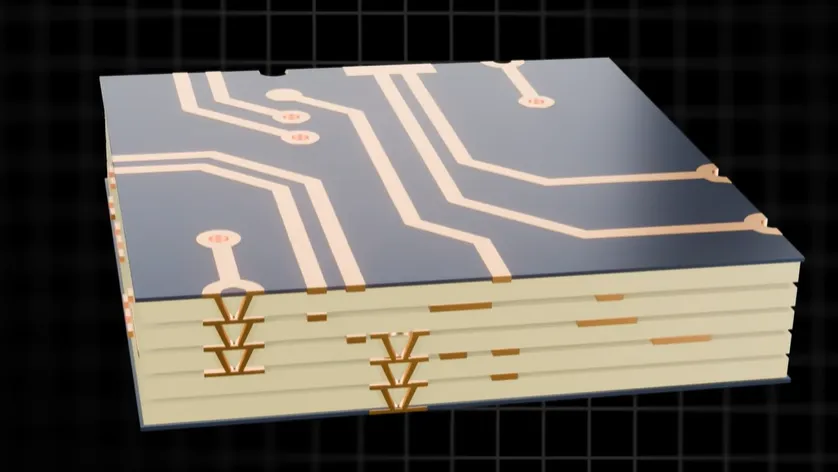
Sequential lamination, also called sequential build-up, constructs HDI boards layer by layer. After each core or sub-laminate is processed, additional dielectric and copper foils are added, laser-drilled, and plated. This approach permits blind and buried microvias at multiple levels and supports both staggered and stacked configurations.
Registration accuracy across successive lamination cycles is critical. Material movement, copper-density imbalance, and thermal expansion differences can shift features beyond the allowed tolerance, leading to via-to-pad misalignment. Controlled-impedance layers are typically defined during these build-up stages so that dielectric thickness and trace geometry remain consistent through the final press cycles.
Signal Integrity Gains from Shorter Paths and Reduced Parasitics
Because microvias eliminate the long stubs of conventional through-hole vias, return-path discontinuities and impedance discontinuities are minimized. Lower parasitic inductance and capacitance improve rise-time integrity and reduce crosstalk between adjacent high-speed pairs. Thin dielectrics further shorten vertical interconnect length and allow tighter coupling control for differential pairs.
In high-frequency designs the combination of microvias and fine-line geometry supports higher data rates while keeping the overall board outline compact. Controlled-impedance routing is routinely applied on both outer and inner build-up layers to maintain consistent characteristic impedance across the signal path.
Critical DFM Considerations for Reliable Microvia Stacking and Fine-Line Routing
Design-for-manufacturability rules for HDI focus on via reliability and yield. Stacked microvias concentrate mechanical stress at the interfaces between successive via levels; staggered microvias distribute that stress and generally offer higher long-term reliability under thermal cycling. When stacking is required, each via should be fully filled and planarized before the next dielectric is applied.
Capture-pad diameter must provide sufficient annular ring after laser drill and registration tolerance. Fine-line traces demand adequate copper adhesion and etch-factor compensation to prevent undercut or necking. Dielectric material selection should match the coefficient of thermal expansion of the copper and of any dense component packages to reduce warpage and via cracking risk. Early review of stack-up, via type, and copper balance against fabricator process capability prevents costly redesigns after prototype runs.
Common Production Risks and Failure Modes in HDI PCB Manufacturing
Incomplete laser ablation leaves dielectric residue that impedes plating and creates open or high-resistance vias. Over-aggressive laser energy can damage underlying pads or cause sidewall roughness that traps plating solution. In sequential lamination, insufficient resin flow or improper press parameters produce voids or delamination at build-up interfaces.
Stacked microvias are susceptible to interfacial cracking under repeated thermal stress if the fill material and plating quality are marginal. Fine-line etching variations can create opens or excessive resistance on critical nets. Material CTE mismatch between thin dielectrics and heavy copper planes contributes to board warpage that affects subsequent assembly yield. These risks are mitigated by process-window qualification, in-process AOI and X-ray inspection, and adherence to documented DFM guidelines for via aspect ratio, pad size, and copper distribution.
| Parameter | Standard Through-Hole PCB | HDI PCB (Typical) |
|---|---|---|
| Via diameter | ≥ 200–300 µm | ≤ 150 µm (laser microvia) |
| Aspect ratio | Up to 8–10:1 | ≤ 0.75–1:1 |
| Minimum trace/space | 100–125 µm | 50–75 µm or finer |
| Layer construction | Single lamination | Sequential build-up |
| Typical max layers | 12–16 (conventional) | Up to 20 with microvias |
| Primary density driver | Through vias & larger pads | Microvias & fine lines |
High-Density Applications in Compact High-Performance Electronics
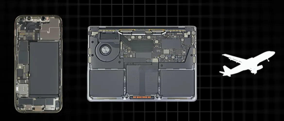
HDI technology is applied wherever board real estate is limited and electrical performance cannot be compromised. Smartphones and tablets rely on multiple microvia levels to route high-pin-count processors and memory packages. Medical devices use the same density advantages to integrate sensors, processors, and wireless modules inside small enclosures while meeting reliability and signal-integrity requirements. Aerospace and defense systems adopt HDI for reduced weight, improved vibration resistance, and controlled-impedance high-speed links.
In each case the combination of shorter interconnect paths, higher routing density, and sequential build-up enables functional performance that would otherwise require larger or multi-board solutions.
Fabrication Capabilities Supporting Up to 20-Layer HDI Boards
Production support covers boards up to 20 layers with both stacked and staggered microvia configurations. Controlled-impedance routing is available on designated layers, and a range of advanced surface finishes can be applied to meet assembly and environmental needs. Instant project pricing is obtained through the online quote tool; detailed process specifications appear on the dedicated HDI PCB page, with application notes available in the medical-devices PCB section.
FAQ
Q1: How do microvias improve signal integrity and speed in HDI PCBs compared to standard vias?
A1: Microvias improve signal integrity and transmission speed by shortening electrical paths, reducing parasitic inductance and capacitance, and minimizing signal loss and crosstalk compared to traditional through-hole vias. Their smaller size also enables denser routing and better performance in high-speed, high-frequency PCB designs.
Q2: What is the maximum layer count and microvia configuration supported for HDI PCB fabrication?
A2: The HDI PCB fabrication capabilities support up to 20-layer boards with both stacked and staggered microvia configurations, along with controlled impedance routing and advanced surface finishes.
Q3: Which compact high-performance applications benefit most from HDI PCB technology?
A3: HDI PCB technology is widely used in compact, high-performance applications such as smartphones, tablets, medical devices, aerospace electronics, and other miniaturized systems requiring high component density, fast signal transmission, and reliable multilayer interconnections.
Q4: What DFM rules reduce the risk of stacked-microvia failure under thermal cycling?
A4: Prefer staggered microvias when possible. When stacking is required, ensure complete via fill and planarization at each level, maintain adequate capture-pad annular ring, select dielectrics with matched CTE, and verify the full stack-up against the fabricator's qualified process window before tape-out.
Q5: How does sequential lamination affect registration and yield in multilayer HDI boards?
A5: Each additional build-up cycle introduces potential material movement and copper-density imbalance. Tight control of press parameters, copper balancing, and optical or X-ray registration targets is required to keep microvia-to-pad alignment within tolerance and to avoid opens or shorts that reduce yield.
This is an HDI PCB — a high-density interconnect board designed for advanced miniaturization.
Built with microvias, fine lines, and thin dielectrics, it enables more components in less space.
Its biggest advantage is density: it supports higher I/O counts and faster signal transmission without increasing board size.
It also improves electrical performance, reducing crosstalk and enhancing reliability in high-speed designs.
And with sequential lamination and laser drilling, assembly remains precise even for complex multilayer structures.
You'll find HDI PCBs in smartphones, tablets, medical devices, aerospace systems, and any product where compactness and performance are critical.
We support up to 20-layer HDI fabrication, stacked and staggered microvias, controlled impedance routing, and advanced surface finishes.
Feel free to explore specifications, capabilities, and stack-up details on our platform whenever you need them.





