 00:58
00:58
HDI Technology
High Density Interconnect (HDI) technology represents a cornerstone of modern printed circuit board (PCB) design, enabling the creation of compact, high-performance electronics by incorporating finer lines, smaller vias, and multiple layers of interconnections. This approach allows engineers to pack more functionality into smaller footprints, making it essential for applications in consumer electronics, automotive systems, medical devices, and telecommunications equipment. For professionals and hobbyists searching for HDI Technology, this tag serves as a curated resource that delves into the intricacies of designing and manufacturing these advanced PCBs, addressing common challenges such as signal integrity, thermal management, and cost optimization. Understanding HDI Technology begins with its key features, including microvias, buried vias, and sequential lamination processes, which facilitate higher circuit density without compromising reliability. Users often seek practical guidance on implementing HDI in their projects, such as selecting appropriate substrate materials or optimizing layer stackups to minimize electromagnetic interference. Best practices include adhering to IPC standards for via filling and plating to ensure durability, as well as using simulation tools early in the design phase to predict performance issues. These insights can significantly reduce prototyping iterations and production costs, particularly in high-volume manufacturing scenarios where space constraints are critical. For those looking to apply HDI Technology in real-world scenarios, the articles under this tag offer in-depth explorations of case studies, from integrating HDI in wearable devices to enhancing data rates in high-speed computing. By reviewing these resources, designers can gain actionable strategies for overcoming fabrication limitations and achieving superior electrical performance. Whether you are troubleshooting a specific HDI implementation or seeking to advance your PCB expertise, the content here provides the technical depth needed to innovate effectively in electronics design.
Video Guide
Technical Articles
What Is HDI PCB? Meaning, Applications, and Technology Overview
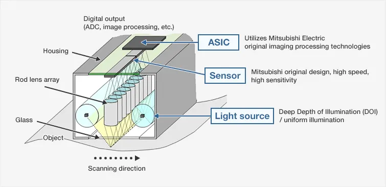
CMOS Image Sensor PCB Design Guide: Architecture, Performance Optimization, and Manufacturing Considerations
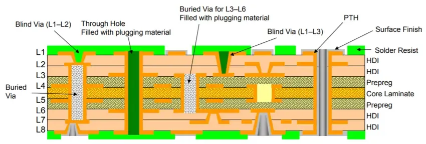
Miniaturized HDI PCB: Design and Manufacturing for Small Form Factor Electronics
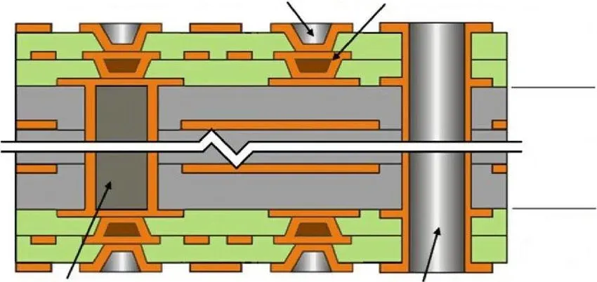
Advanced HDI PCB: Materials, Manufacturing, Design, and Interconnect Technology

Building Insights from a Polaroid Photo Frame Hack – PCB Reverse Engineering Journey
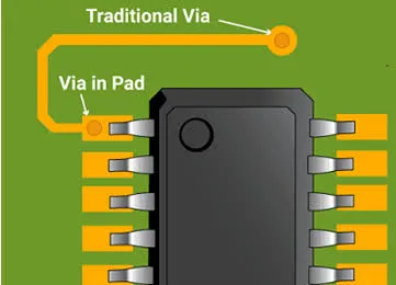
Via-in-Pad vs Traditional Via Routing for HDI PCB
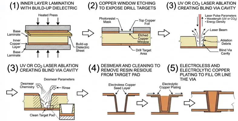
HDI Laser Drilling Mistakes That Affect Manufacturing Yield
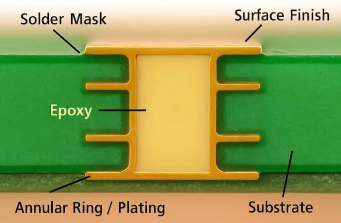
Resin Filled Via vs Copper Filled Via HDI: What Is the Difference?
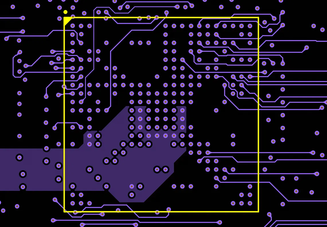
Basics of routing with BGA packages
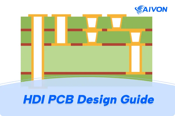
HDI Design Guide: Stackup Principles, Microvia Reliability and High-Density Routing Guide

Moto 360 Gen 2: Design and Hardware Updates

History of Smartwatches and Early Watch Operating Systems

Moto 360 Second Gen: Small Updates, Missing Key Features
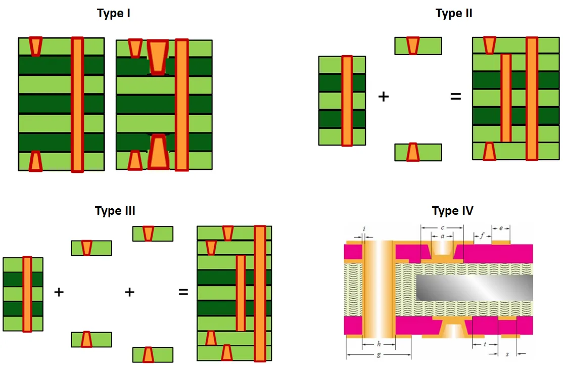
The Future of HDI PCBs: Trends in Miniaturization, Materials, and Manufacturing
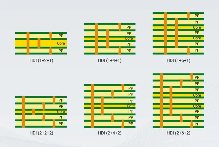
HDI PCB Stack Up Design: Optimizing Layer Count and Signal Routing
HDI PCB Manufacturing Guide: Microvia Technology, Structures and Capabilities
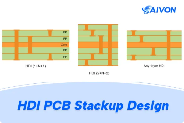
HDI Stackup Design Guide: 1+N+1, 2+N+2, and Any-Layer
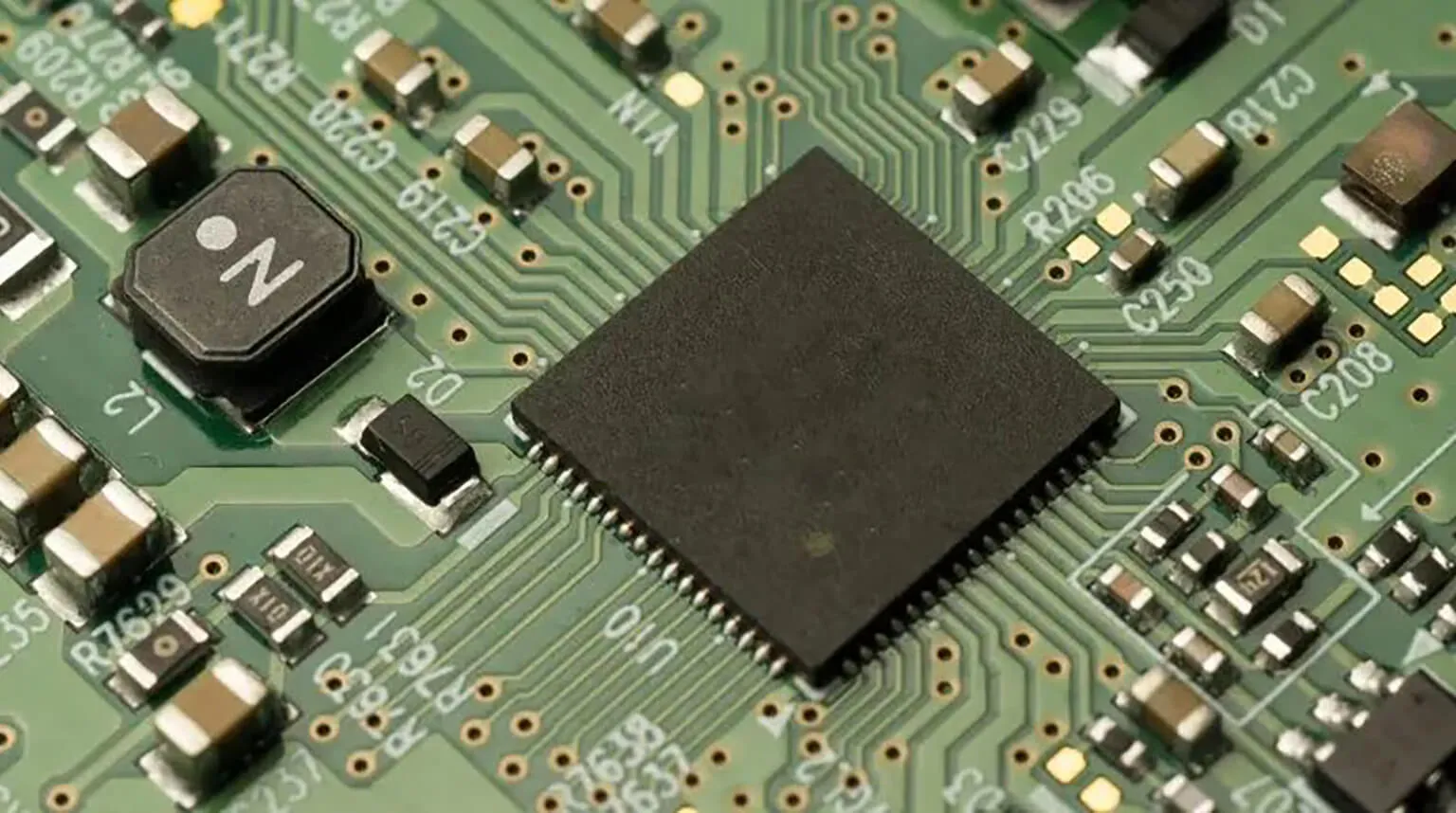
HDI PCB Assembly: The Ultimate Guide to Materials, Stack-Up Structures, DFM & Best Practices
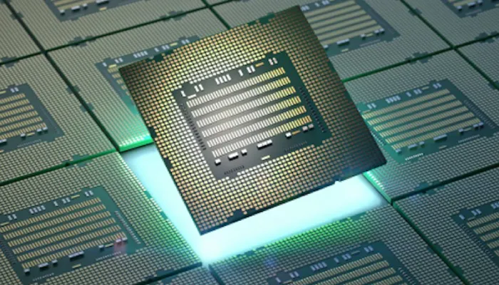
HDI PCB Applications: Powering Miniaturization, Performance, and Reliability Across Industries