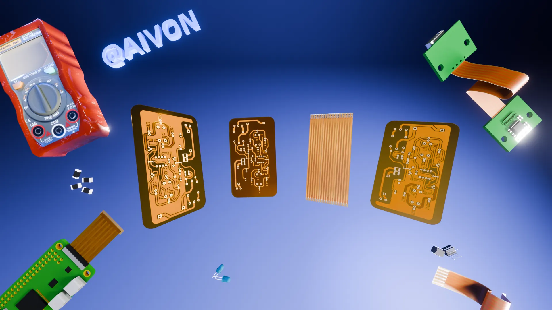
What Is an HDI PCB? High Density Interconnect Explained
WHAT THIS VIDEO COVERS
This video explains HDI PCB technology and why it is the preferred choice when board size, component density, and electrical performance must be optimized together. It covers the use of microvias that connect layers directly without through-holes, extremely fine traces, and advanced layer stack-ups that allow more circuitry in thinner boards while maintaining signal integrity.
The content highlights how HDI structures shorten routing paths, reduce parasitic effects, and support higher I/O counts in modern devices. Viewers learn exactly when standard multilayer PCBs are no longer sufficient and why HDI becomes the engineering solution for space-constrained applications.
Practical examples include smartphones, wearables, and other high-density consumer electronics. The video also clarifies manufacturing considerations such as precision drilling, plating, and lamination that are required to produce reliable HDI boards. For immediate pricing on HDI designs, use our PCB quote tool. Engineers looking for production-ready HDI solutions can explore our dedicated HDI PCB capabilities or request a PCB.
KEY HIGHLIGHTS
- Microvias and fine traces enable significantly higher connection density without increasing board size.
- Direct layer-to-layer connections shorten signal paths and improve integrity compared with traditional through-hole vias.
- HDI technology supports thinner, higher-layer-count boards ideal for smartphones, wearables, and compact industrial electronics.
FAQ
Q1: How do microvias in HDI PCBs improve signal integrity compared with standard vias?
A1: Microvias connect layers directly without drilling through the entire board. This shortens signal paths, reduces parasitic inductance and capacitance, and minimizes signal loss and crosstalk — especially important in high-speed designs.
Q2: When should a design move from a standard multilayer PCB to an HDI PCB?
A2: Switch to HDI when board space is extremely limited, component density is very high, or the design requires thinner profiles with more layers while maintaining strong signal integrity. Typical triggers include smartphones, wearables, and compact industrial modules where conventional through-hole vias no longer fit the size or performance requirements.
Q3: What manufacturing tolerances are required to produce reliable HDI boards?
A3: Reliable HDI production demands laser-drilled microvias (usually 0.1 mm or smaller), fine-line etching below 75 µm, precise lamination control for stacked or staggered vias, and advanced plating processes to ensure via reliability and thermal performance.
Why do some PCBs look clean, compact, and incredibly dense?
That's often an HDI PCB.
HDI stands for High Density Interconnect.
It's a PCB technology designed to pack more connections into less space.
HDI boards rely on extremely small vias and very fine traces.
These microvias connect layers directly, without passing through the entire board.
Because of this, routing becomes shorter, tighter, and more efficient.
Signals travel more directly, improving signal integrity and electrical performance.
HDI structures also allow more layers to be stacked into thinner boards.
This makes it possible to design compact layouts without sacrificing functionality.
That's why HDI is widely used in smartphones, wearables, and other space-constrained electronics.
So HDI needs precision, used only when size, performance, and density matter.