Introduction
VR headsets demand PCBs that pack high performance into minimal space to enhance user comfort and immersion. Engineers face the challenge of VR headset PCB miniaturization while maintaining signal integrity, thermal management, and reliability under constant motion. As VR devices evolve toward lighter, sleeker designs, small PCB design for VR requires innovative techniques like high-density interconnects and precise component placement. This article explores proven methods to achieve compact layouts without compromising functionality. Key strategies include HDI PCB for VR headsets, microvias in VR PCBs, and optimized component placement for VR headsets.
Miniaturization not only reduces weight but also shortens signal paths, minimizing latency critical for seamless VR experiences. Traditional PCBs struggle with the density needed for processors, sensors, and displays in headsets. Advanced fabrication allows stacking layers efficiently, enabling feature-rich boards in footprints under 50 square centimeters. These techniques align with the push for untethered, all-day wearable VR.
Why Miniaturization Matters for VR Headset PCBs
VR headset PCB miniaturization directly impacts user experience by reducing bulk and improving ergonomics. Lighter headsets prevent neck strain during extended sessions, while compact boards free space for larger batteries or optics. High-density designs support more sensors for precise tracking, essential for 6DoF motion. Small PCB design for VR also enhances heat dissipation in confined enclosures, preventing throttling of high-speed chips.
From an engineering perspective, miniaturization addresses electromagnetic interference challenges in dense layouts. Shorter traces reduce crosstalk and attenuation, preserving bandwidth for 8K displays and eye-tracking. Reliability under vibration demands robust interconnects, as headsets endure daily wear. Cost efficiency emerges too, as smaller boards use less material and streamline assembly.
Market trends amplify the need, with standalone VR pushing for smartphone-like form factors. Engineers must balance density with manufacturability to avoid yield losses. Ultimately, effective VR headset PCB miniaturization unlocks next-generation devices that blend portability with power.
Core Technical Principles of PCB Miniaturization
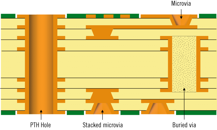
HDI PCB for VR headsetFs leverages multiple build-up layers to achieve finer features than standard multilayers. These boards employ microvias, typically under 150 microns, stacked or staggered for vertical interconnects. Laser-drilled vias connect inner layers precisely, enabling trace widths below 50 microns. This structure supports ball grid arrays with 0.4mm pitch, packing thousands of I/Os into small areas.
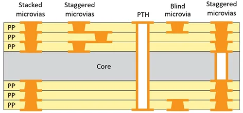
Microvias in VR PCBs form the backbone of density, with blind and buried types minimizing via fields. Type III HDI, per industry guidelines, uses filled or copper-plated vias for mechanical strength. Sequential lamination builds layers incrementally, controlling aspect ratios under 1:1 for reliable plating. These principles reduce board thickness to 0.6mm or less, ideal for slim headsets.
Component placement for VR headsets optimizes real estate through fine-pitch components and embedded passives. Decoupling capacitors nestle under BGAs, while flip-chip dies mount directly on substrates. Thermal vias channel heat from hotspots, maintaining junction temperatures below limits. Signal routing follows controlled impedance rules, with differential pairs for high-speed interfaces like DisplayPort.
Substrate selection influences miniaturization viability, favoring low-CTE materials for warpage control. Thin cores, around 50 microns, pair with resin-coated copper for buildup. Prepreg thickness tunes to 30 microns per layer, compressing stackups. These mechanisms ensure HDI boards withstand reflow cycles without delamination.
HDI PCB Technology in Depth
HDI PCB for VR headsets starts with core selection, often 2–4 layers, then adds microvia layers on both sides. Every-add process fabricates one microvia layer at a time, using photosensitive dielectrics for via patterning. This yields densities over 100,000 pads per square inch, surpassing standard FR-4 capabilities. Laser ablation forms vias cleanly, followed by electroless copper and electroplating for barrel fill,showcasing how advanced HDI PCB applications are powering miniaturization and performance in today’s hardware.
Microvias in VR PCBs demand tight tolerances, with via-in-pad designs routing signals through components. Staggered vias offset positions to avoid drill breakout, enhancing yield. Filled vias, electroplated solid, provide planar surfaces for outer traces. IPC-6016 outlines qualification for these boards, specifying electrical and mechanical tests like thermal cycling.
Layer count in HDI for VR typically reaches 8–12, with any-layer vias in advanced Type IV configs. This interconnects IMUs, SoCs, and PMICs seamlessly. Dielectric constants below 3.5 minimize delay, crucial for low-latency VR. Fabrication windows tighten to 25-micron lines and spaces, pushing DFM limits.
Advanced Component Placement Strategies
Component placement for VR headsets prioritizes central processors and sensors near edges for balanced mass. Fine-pitch QFNs and LFPs occupy core areas, with 0201 passives filling gaps. Fanout from BGAs uses dogbone escapes, microvias fanning out to planes. This layout shortens critical nets, reducing EMI susceptibility.
Thermal management integrates into placement, grouping heat sources over ground planes. Vias-in-pad conduct to inner copper pours, spreading flux. Embedded coins or heat spreaders handle hotspots from GPUs. Simulations verify paths, ensuring gradients stay under 20°C across the board.
Power delivery networks demand distributed caps, placed within 1mm of pins. Microvias stack to feed planes, minimizing inductance. For VR, this supports transient currents from OLED drivers. Layout tools enforce rules like same-net spacing to prevent shorts in dense fields.
Small PCB design for VR incorporates 3D stacking, like PoP for memory over SoC. This halves footprint while preserving bandwidth. Underfill secures dies against shock, vital for head-mounted use. These strategies yield boards under 40x40mm, fitting temple arms snugly.
Practical Best Practices for Implementation
Begin small PCB design for VR with stackup planning, targeting 0.8mm total thickness. Simulate impedance early, adjusting dielectric for 100-ohm pairs. Route high-speed first, using length matching within 5 mils. Microvias in VR PCBs route under components, freeing surface for passives.
Fabrication partners must support laser via drilling and sequential build-up. Specify via fill per IPC-6016 to ensure planarity. Panel utilization optimizes cost, with fiducials for alignment. Post-laminate etch controls linewidth variation under 10%.
Assembly for HDI PCB VR headsets uses split stencils for stepped profiling. Jet printing applies paste precisely on 0.3mm pads. Reflow profiles follow J-STD-020, preconditioning for MSL3 components. X-ray inspects BGA voids, targeting under 25%.
Testing verifies miniaturization integrity through flying probe for opens/shorts. Thermal shock per IPC-TM-650 assesses reliability. Signal integrity sweeps confirm eye diagrams at 10Gbps. These practices ensure field performance in dynamic VR environments.
Challenges in VR Headset PCB Miniaturization and Solutions
Warpage plagues thin HDI stacks due to CTE mismatch, bowing up to 0.75% unconstrained. Symmetric buildups and low-flow prepregs counteract this, per IPC-6012 guidelines. Carrier tabs during fab maintain flatness for assembly.
Reliability under flexing demands robust microvias, tested via IPC-TM-650 cyclic bend. Copper ductility and via taper prevent cracking. Solder joint integrity follows J-STD-001, with underfill for fine-pitch.
Signal loss in high-density routing requires low-loss dielectrics. Serpentine patterns equalize lengths for clocks. Shielding vias isolate aggressors. These mitigations sustain VR performance.
Conclusion
VR headset PCB miniaturization transforms bulky prototypes into sleek wearables through HDI, microvias, and precise placement. Engineers achieve densities rivaling mobiles while meeting reliability standards. Small PCB design for VR balances space, speed, and stability for immersive experiences. Adopting these techniques streamlines development, cutting iterations. Future iterations will push finer features, driven by compute demands.
FAQs
Q1: What role do microvias play in VR headset PCB miniaturization?
A1: Microvias in VR PCBs enable vertical connections in HDI stackups, reducing board area by eliminating large via fields. They support blind and buried structures for inner layer access, achieving trace densities over 50 microns. Laser drilling ensures precision, with plating for conductivity. This technique per IPC-6016 enhances small PCB design for VR without expanding footprints.
Q2: How does HDI PCB for VR headsets improve component placement?
A2: HDI PCB for VR headsets allows tighter component placement by providing high-density routing under BGAs. Microvias fan out pins efficiently, nesting passives nearby. This minimizes loop inductance for power stability. Sequential lamination builds support fine features, optimizing space in compact enclosures.
Q3: What are key considerations for small PCB design in VR applications?
A3: Small PCB design for VR prioritizes thermal vias and impedance control amid density. Stack thin layers with low-CTE materials to curb warpage. Route differentially for sensor data integrity. Test per J-STD-001 ensures assembly yield. These steps deliver reliable VR headset PCB miniaturization.
Q4: Why use stacked microvias in high-density VR PCBs?
A4: Stacked microvias in VR PCBs connect multiple layers compactly, ideal for 12-layer HDI. They are often staggered to prevent alignment issues, boosting yield. Filled variants planarize for outer traces. This supports VR headset PCB miniaturization with minimal thickness increase.
References
IPC-6016 — Qualification and Performance Specification for High Density Interconnect (HDI) Printed Boards. IPC, 2010
IPC-6012E — Qualification and Performance Specification for Rigid Printed Boards. IPC, 2015
J-STD-001H — Requirements for Soldered Electrical and Electronic Assemblies. IPC, 2018
J-STD-020E — Moisture/Reflow Sensitivity Classification for Nonhermetic Surface Mount Devices. JEDEC, 2014


