Introduction
Marine navigation systems rely on printed circuit boards (PCBs) to power critical components like radar displays, GPS modules, and autopilot controllers. In harsh marine environments, factors such as constant vibration, high humidity, saltwater corrosion, and temperature fluctuations demand robust power distribution strategies. Poor power management can lead to signal degradation, intermittent failures, or complete system downtime during critical voyages. Optimizing marine PCB power integrity ensures stable voltage delivery, minimizes electromagnetic interference (EMI), and enhances overall system reliability. This guide explores key techniques for engineers designing PCBs for navigation applications, focusing on voltage drop mitigation, grounding, power planes, and EMI control. By applying these principles, designers can create boards that withstand marine rigors while meeting performance specifications.
The Importance of Power Distribution in Marine Navigation PCBs
Power distribution forms the backbone of any marine navigation PCB, where uninterrupted supply to high-speed digital circuits and analog sensors is essential. Navigation systems operate in dynamic conditions, including electromagnetic noise from onboard motors and radio frequency interference from communication antennas. Compromised power integrity manifests as voltage sags, ground bounces, or ripple, which corrupt sensor data and navigation accuracy. Engineers must prioritize marine PCB power integrity to prevent cascading failures that could endanger vessels. Standards like IPC-2221 provide foundational guidelines for designing power networks resilient to environmental stresses. Ultimately, effective power handling directly correlates with the longevity and precision of marine electronics.
In marine settings, power demands vary widely, from low-power microcontrollers to power-hungry RF transceivers. Voltage instability exacerbates issues in compact PCBs typical of navigation consoles. Reliable distribution reduces failure rates, lowers maintenance costs, and complies with reliability benchmarks. Designers face unique challenges like conductive corrosion paths from salt ingress, which amplify leakage currents and ground potential differences.
Core Principles of Voltage Drop in Marine PCBs
Voltage drop, or IR drop, occurs when current flows through resistive traces or planes, reducing available voltage at load points. In marine navigation PCBs, long power routing paths and high currents from illumination backlights or motor drivers intensify this effect. Accurate voltage drop calculation PCB starts with modeling resistance using sheet resistivity formulas, where R = ρ * (L / W), ρ being the copper resistivity adjusted for temperature. Engineers simulate worst-case scenarios, factoring in ambient temperatures up to 70°C and derating for aging. Multi-layer stacks help by shortening paths, but splits in planes demand careful via placement.
To compute voltage drop precisely, divide the PCB into segments and sum drops across each: V_drop_total = Σ (I_segment * R_segment). Temperature rise from self-heating follows P = I2R, influencing resistivity via α * ΔT correction, where α is copper's temperature coefficient. In marine applications, vibration-induced microcracks increase resistance over time, necessitating margins of 5-10% below component minimum voltages. Validation through DC analysis tools confirms compliance before fabrication.

Parasitic inductance from vias and traces contributes to dynamic drops during transients, critical for switching regulators in navigation systems. Minimizing loop areas reduces L = μ * (area / length), preserving fast edge integrity.
Grounding Techniques for Marine Navigation PCBs
Grounding techniques marine PCB address noise coupling and return path integrity, vital in EMI-prone marine environments. A solid ground plane provides low-impedance returns, distributing currents evenly and shielding sensitive signals. However, in navigation PCBs with mixed analog-digital sections, partitioned grounds prevent digital noise from polluting analog references. Star grounding converges returns at a single point near the power entry, ideal for low-frequency analog circuits like gyroscopes. Mesh grounding, with dense stitching vias, suits high-speed digital domains by minimizing loop inductance.
Implement grounding by dedicating inner layers to ground, using vias every 1/20th wavelength of highest frequency for RF containment. In marine setups, corrosion-resistant coatings protect ground planes, but engineers must avoid ground loops from chassis connections that induce hum from alternators. IPC-A-610 outlines acceptability criteria for ground vias and plating integrity post-fabrication. Hybrid approaches, like guarding analog grounds with moats tied at one end, balance isolation and continuity.
Return currents follow the path of least impedance, so proximity to signals dictates coupling levels. Testing involves injecting common-mode noise to verify rejection ratios.
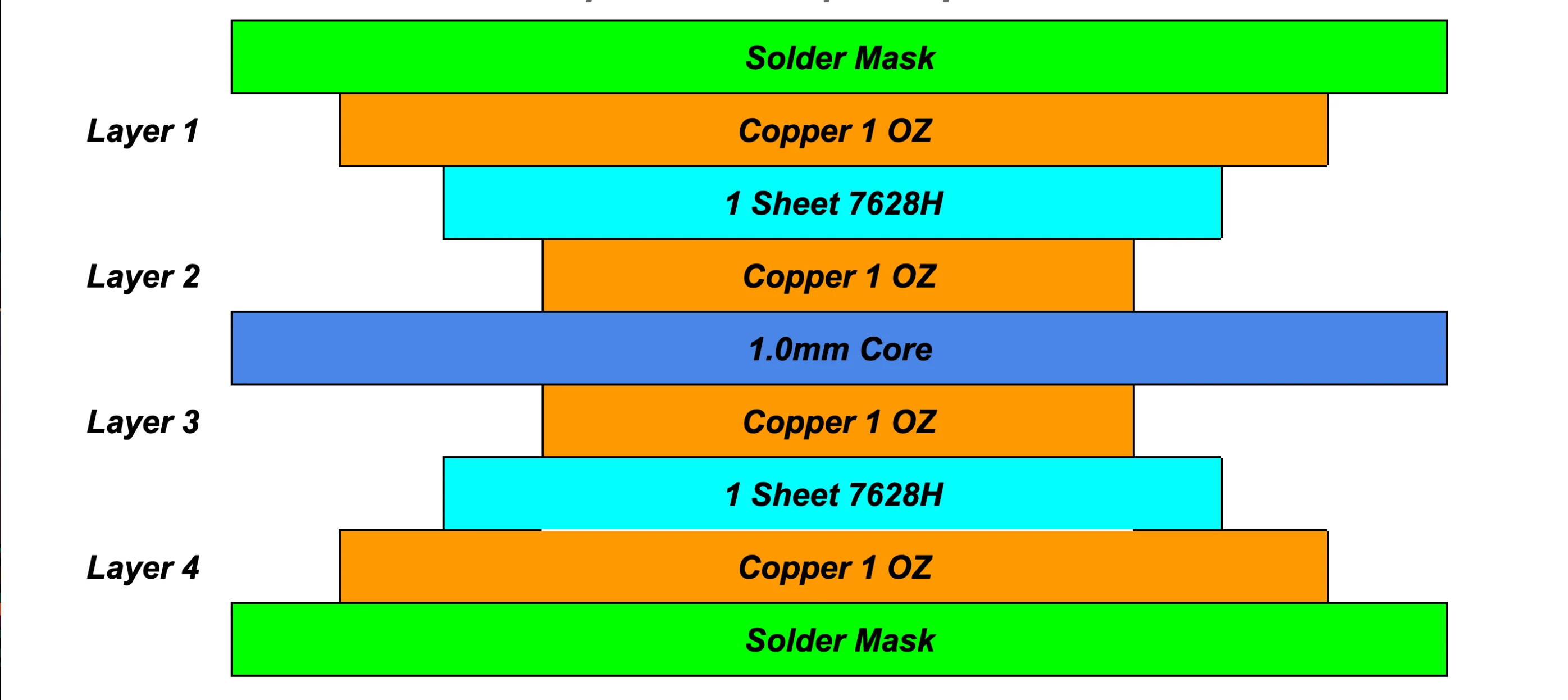
Power Plane Design for Marine Navigation Systems
Power plane design marine navigation optimizes current spreading and voltage stability across the board. Solid planes offer lowest resistance, calculated as R_plane = ρ * (L / W) * (t / thickness factor), where thickness accounts for skin effect at high frequencies. For multi-rail supplies common in navigation gear, split planes require inter-plane capacitors at splits to bridge high-frequency returns. Core thickness influences capacitance between power-ground pairs, C = ε * A / d, aiding decoupling.
Strategically place power entry points centrally to equalize drops, and use spoke vias for even distribution. In marine PCBs, thicker copper (2-3 oz) combats thermal cycling stresses, per IPC-6012 performance specs. Avoid narrow necks in planes that create bottlenecks during peak loads from display refreshes.
Plane splits demand careful alignment under ICs to prevent mid-plane via inductance spikes. Thermal reliefs in vias prevent solder voids while maintaining conductivity.
Strategies for EMI Reduction in PCB Power Distribution
EMI reduction PCB power tackles radiated and conducted emissions from switching noise and plane resonances. Decoupling capacitors, placed <1mm from IC pins, shunt high-frequency currents, with values selected via f = 1/(2π√(LC)). Ferrite beads on power lines attenuate conducted EMI above 10MHz without dropping DC voltage. Guard traces alongside power lines absorb edge-coupled fields.
Plane resonances occur at quarter-wavelength modes, mitigated by stitching capacitors or slots perpendicular to flow. In marine navigation, where antennas are nearby, cavity models predict fields between planes, guiding cutout placements. Ground isolation slots halt surface waves, but require bypasses for returns. J-STD-001 emphasizes soldering quality for EMI filters to ensure low parasitics.
Shielding cans over noisy sections complement PCB-level fixes, grounded at multiple points.
Best Practices for Implementation
Integrate these elements during schematic capture: assign net classes for power with width rules scaling by current density <30A/mm2. Stackup planning prioritizes power-ground adjacency for impedance control, targeting 50Ω for signals but lower for PDNs. Simulate full-board IR drop and transient response, iterating until margins hold under Monte Carlo variations for trace etch tolerances.
Fabrication inputs specify controlled impedance for power traces and X-ray inspection for via barrels. Assembly verification includes power-up sequencing to avoid latch-up in marine-grade components. Field testing simulates wave motion with shakers to validate dynamic integrity.
Post-deployment, thermal imaging spots hotspots indicating distribution flaws.
Troubleshooting Common Issues
Engineers encounter voltage droops from undersized planes, diagnosed by probing loads during stress tests. Ground bounces appear as oscilloscope glitches, fixed by adding return vias near IO pins. EMI failures in compliance scans trace to un-decoupled regulators; spectrum analysis pinpoints frequencies for targeted fixes. Corrosion manifests as creeping resistance, countered by conformal coatings per IPC standards.
Iterative prototyping with short runs refines designs before volume production.
Conclusion
Optimizing power distribution in marine navigation PCBs demands a holistic approach encompassing voltage drop calculation PCB, grounding techniques marine PCB, power plane design marine navigation, and EMI reduction PCB power. These strategies ensure marine PCB power integrity amid environmental adversities, safeguarding navigation reliability. Adhering to established standards and simulation-driven design yields robust outcomes. Engineers equipped with these insights can deliver systems that perform flawlessly on the open sea. Prioritize early integration of these practices to minimize redesign cycles and enhance product lifespan.
FAQs
Q1: How do you perform voltage drop calculation PCB for marine applications?
A1: Voltage drop calculation PCB involves segmenting power paths and applying R = ρ * L / (W * t), summing I * R products with temperature corrections. Factor marine currents from displays and radios, aiming for <5% drop. Simulate DC sweeps including derating for 85°C operation. Validate with measurements under load to confirm margins.(62 words)
Q2: What are effective grounding techniques marine PCB?
A2: Grounding techniques marine PCB include solid planes for digital returns and partitioned analog sections with star points. Stitch vias densely to lower impedance, avoiding loops from hull grounds. Use inner layers for shielding, per IPC guidelines. Test for noise coupling with injection probes to refine.(54 words)
Q3: Why is power plane design marine navigation critical?
A3: Power plane design marine navigation ensures uniform voltage amid vibrations and corrosion. Solid or split planes with central feeds minimize IR drops and resonances. Thicker copper handles thermal cycles, maintaining integrity. Simulations predict performance before build.(48 words)
Q4: How to achieve EMI reduction PCB power in navigation systems?
A4: EMI reduction PCB power uses close decoupling, ferrites, and stitching caps to shunt noise. Align splits carefully and add guard traces. Compliance testing identifies fixes like slots for wave suppression. This preserves signal fidelity near antennas.(52 words)
References
IPC-2221G — Generic Standard on Printed Board Design. IPC, 2022
IPC-6012E — Qualification and Performance Specification for Rigid Printed Boards. IPC, 2015
IPC-A-610H — Acceptability of Electronic Assemblies. IPC, 2020
J-STD-001H — Requirements for Soldered Electrical and Electronic Assemblies. IPC, 2020


