 00:58
00:58
Copper Microvias
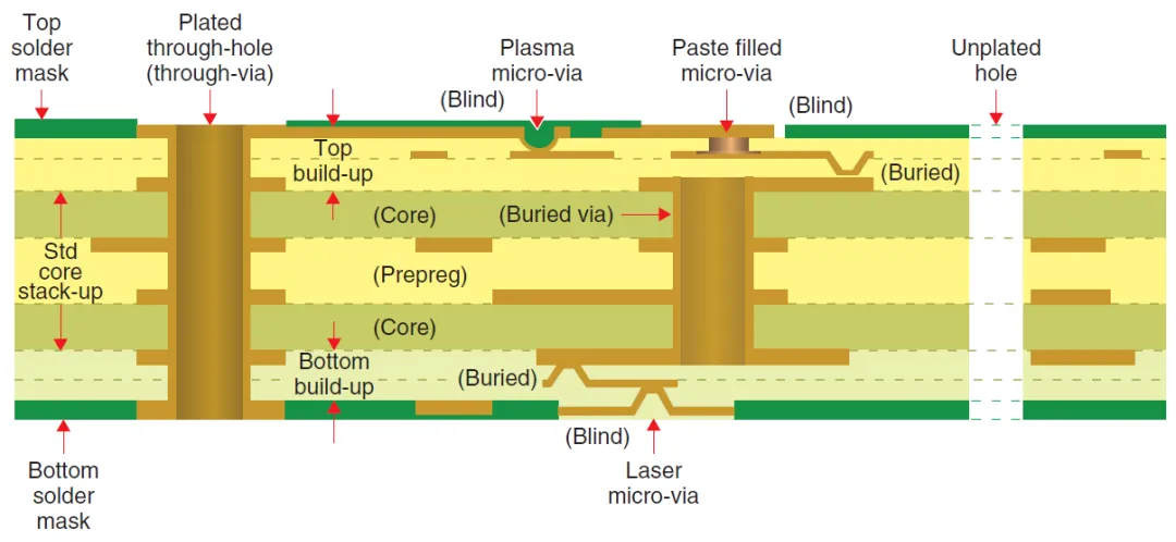
Copper microvias represent a critical advancement in printed circuit board (PCB) design, enabling higher density and improved performance in modern electronics. These small, laser-drilled vias, typically with diameters under 150 micrometers, are plated or filled with copper to facilitate reliable electrical connections between layers in multilayer PCBs. They are essential for high-density interconnect (HDI) technologies, where space constraints demand compact routing without sacrificing signal integrity or thermal management. For engineers and designers searching for information on copper microvias, this tag serves as a comprehensive resource, covering everything from fundamental concepts to advanced implementation strategies. Understanding copper microvias begins with their manufacturing process, which often involves precise laser ablation followed by copper electroplating to ensure void-free filling and minimal resistance. This approach not only reduces the overall board size but also enhances reliability in applications such as smartphones, automotive electronics, and medical devices. Key benefits include better signal propagation at high frequencies, reduced parasitic capacitance, and improved heat dissipation compared to traditional through-hole vias. However, achieving optimal results requires attention to best practices, such as selecting appropriate aspect ratios to avoid defects like cracking or delamination during thermal cycling. Designers should also consider stack-up configurations that balance layer count with microvia placement to prevent manufacturing yield issues. For those tackling real-world challenges, practical insights include guidelines for simulation tools that model microvia performance under stress, as well as troubleshooting common failures like copper migration in humid environments. Articles under the Copper Microvias tag delve into these topics, offering case studies and expert tips to refine your PCB designs. Whether you are optimizing for cost efficiency or pushing the limits of miniaturization, the content here provides actionable knowledge to support your projects effectively.
Video Guide
-
00:58
Technical Articles
Get in Touch
Send Message
- Products & Service
- Company
- About AIVON
- Contact
- News
- Blog
- Certification
-


- Payment
-


2026 AIVON.COM All Rights Reserved