Introduction
In the demanding field of avionics, every gram counts toward achieving optimal aircraft performance. Compact avionics PCB design has become essential for integrating advanced electronics into tight spaces while minimizing overall system weight. Engineers face the challenge of packing high functionality into small form factor avionics PCBs without compromising reliability or signal integrity. This approach not only reduces fuel consumption but also enhances maneuverability in both commercial and military aircraft. As avionics systems evolve with increased processing power and sensor density, lightweight avionics PCB solutions emerge as a critical enabler. The focus on miniaturization aligns with broader aerospace goals of efficiency and sustainability.
Why Miniaturization Matters in Avionics PCBs
Avionics systems operate under extreme conditions, including rapid temperature changes, vibration, and altitude variations, making weight reduction a primary design driver. A lightweight avionics PCB directly contributes to lower aircraft gross weight, which translates to extended range and reduced operational costs. Traditional bulky PCBs limit integration in modern unmanned aerial vehicles and next-generation cockpits, where space is at a premium. High-density interconnect (HDI) PCB for avionics addresses these constraints by enabling more circuitry in less area. Engineers must balance density with thermal dissipation and electromagnetic compatibility to ensure long-term performance. Ultimately, small form factor avionics PCB designs support the industry’s shift toward more autonomous and efficient flight systems.
Core Technical Principles of Compact Avionics PCB Design
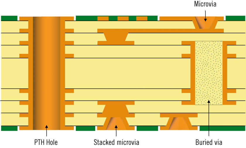
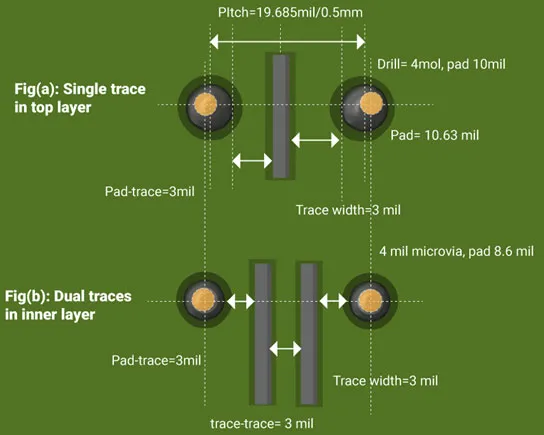
Miniaturization begins with high-density interconnect technology, which uses microvias, blind vias, and buried vias to route signals efficiently across multiple layers. These structures allow trace widths and spaces as fine as 50 microns, far tighter than standard PCBs, facilitating compact layouts. Substrate selection plays a key role, favoring thin dielectrics with low coefficients of thermal expansion to maintain planarity during fabrication. Layer stackups in HDI boards typically incorporate build-up processes, where sequential lamination adds layers with laser-drilled vias for precise interconnections. Signal integrity remains paramount, as reduced dimensions increase risks of crosstalk and impedance mismatches. Adhering to IPC-6012E guidelines ensures qualification for high-reliability applications like avionics.
Material choices further enable weight savings, with low-weight laminates offering dielectric constants optimized for high-frequency signals common in avionics. Copper foil thickness is minimized to 1/2 oz or less in outer layers, reducing overall board mass without sacrificing current-carrying capacity. Via-in-pad designs eliminate unnecessary pads, shrinking footprint areas significantly. These principles collectively allow engineers to achieve board sizes reduced by up to 50 percent compared to conventional designs. However, precise control over aspect ratios during drilling prevents defects like via barrel cracks under thermal stress.
Component Selection for Miniaturized Avionics PCBs
Component selection for miniaturized avionics PCB demands parts with the smallest possible footprints while meeting aerospace-grade reliability. Passive components shift toward 0201 or even 01005 sizes, which occupy minimal board real estate and contribute to lightweight avionics PCB goals. Integrated circuits favor fine-pitch BGAs with 0.4 mm or smaller pitches, enabling dense placement without expanding the board outline. Active devices must exhibit low power consumption to mitigate heat in confined spaces, often incorporating embedded passives within packages. JEDEC J-STD-020E standards guide handling to prevent moisture-induced failures during reflow soldering of these tiny parts. Engineers evaluate derating factors, ensuring components operate well below maximum ratings under combined vibration and thermal loads.
Proximity placement strategies group high-speed signals with their drivers and receivers, minimizing trace lengths in compact avionics PCB design. Decoupling capacitors position as close as possible to power pins, sometimes using array configurations for efficiency. Shielding cans or embedded ground planes address EMI concerns inherent in high-density layouts. Reliability testing verifies solder joint integrity, particularly for bottom-terminated components prone to head-in-pillow defects. This methodical selection process ensures the assembled board meets small form factor avionics PCB requirements without reliability trade-offs.
Best Practices for High-Density Interconnect PCB in Avionics
Start with a robust stackup design that symmetrizes layers to prevent warpage, a common issue in thin, high-layer-count HDI boards. Sequential build-up fabrication allows any-layer vias, maximizing routing density while controlling via capture pad sizes to under 150 microns. Controlled impedance modeling verifies trace geometries against avionics frequency requirements, typically up to several GHz. Thermal vias under hot components channel heat to inner planes, maintaining junction temperatures within limits. IPC-A-600K acceptability criteria guide visual inspections for defects like measling or delamination post-lamination.
Fabrication tolerances tighten to ±0.05 mm for features, necessitating design for manufacturability from the outset. Panelization strategies optimize yield for small boards, using fiducials for precise alignment during assembly. Solder mask application employs photoimageable materials for fine-line definition over traces. Bake-out processes precondition boards per JEDEC guidelines to remove absorbed moisture before assembly. Post-assembly, conformal coatings protect against environmental ingress in avionics enclosures.
Routing follows length-matching rules for differential pairs, with teardrops at vias to reduce stress concentrations. Power distribution networks employ wide planes segmented for isolation, minimizing voltage drops in dense layouts. Design rule checks enforce minimum clearances, adapting to HDI capabilities like 3-N-3 microvia stacking. Simulation tools predict resonance modes, informing cutouts or stitching vias. These practices culminate in lightweight avionics PCB that pass qualification testing for shock and vibration.
Challenges and Mitigation Strategies
High-density interconnect PCB for avionics introduces challenges like via reliability under cyclic loading. Stacked microvias risk cracking if not filled properly, so filled vias with plated caps enhance robustness. Warpage control involves matched CTE materials between cores and build-up films. Aspect ratios stay below 0.8:1 for reliable plating in small vias. Signal loss at high frequencies demands low-loss dielectrics, carefully selected for Dk and Df values.
Assembly processes adapt with low-temperature solders to protect thin traces from reflow damage. Inspection shifts to automated optical systems for 100 percent microvia checks. Functional testing includes boundary scan for inaccessible nets in small form factor avionics PCB. These mitigations ensure the design progresses from prototype to flight-qualified hardware seamlessly.
Conclusion
Compact avionics PCB design revolutionizes weight reduction by leveraging HDI technologies, precise component selection, and rigorous best practices. Engineers achieve substantial size and mass savings while upholding reliability in harsh environments. Key to success lies in integrating standards like IPC-6012E early in the process. As avionics complexity grows, these miniaturized solutions will drive further innovations in aircraft efficiency. Prioritizing logical stackups, material choices, and verification steps yields robust, lightweight systems ready for deployment.
FAQs
Q1: What are the main benefits of high-density interconnect (HDI) PCB for avionics?
A1: HDI enables compact avionics PCB design by using microvias and fine traces to fit more functionality into smaller areas, directly supporting weight reduction. It improves signal integrity for high-speed data and reduces overall board thickness. Reliability remains high when following standards like IPC-A-600K for inspection. This technology is ideal for space-constrained avionics modules.
Q2: How does component selection impact lightweight avionics PCB performance?
A2: Selecting small-footprint components like 0201 passives and fine-pitch BGAs minimizes board size in component selection for miniaturized avionics PCB. Low-profile packages lower center of gravity, aiding vibration resistance. JEDEC J-STD-020E ensures reflow compatibility, preventing defects. Balanced power draw prevents thermal hotspots in dense layouts.
Q3: What stackup considerations are critical for small form factor avionics PCB?
A3: Symmetric layer pairing prevents warpage in small form factor avionics PCB, with thin cores and build-up dielectrics for minimal thickness. Blind and buried vias optimize routing density without through-hole penetration. Impedance control matches avionics signal speeds. Sequential lamination per IPC-6012E supports complex HDI structures reliably.
Q4: Why is via reliability important in compact avionics PCB design?
A4: Vias endure thermal cycling and vibration in compact avionics PCB design, so filled microvias enhance fatigue resistance. Laser drilling achieves small diameters for density, but plating uniformity is key. Standards guide aspect ratios to avoid cracks. Proper stackup sequencing ensures interconnection integrity over the board’s lifecycle.
References
IPC-6012E — Qualification and Performance Specification for Rigid Printed Boards. IPC, 2017
IPC-A-600K — Acceptability of Printed Boards. IPC, 2020
JEDEC J-STD-020E — Moisture/Reflow Sensitivity Classification. JEDEC, 2014


