Introduction
High-density interconnect (HDI) PCBs represent a pivotal advancement in automotive electronics, enabling the integration of complex systems within limited space. As vehicles incorporate more sensors, processors, and control units, HDI PCB automotive applications become essential for achieving higher functionality and performance. These boards support the demands of modern vehicles, particularly in advanced driver assistance systems (ADAS), where compactness and signal integrity are non-negotiable. Engineers face challenges like extreme temperatures, vibrations, and electromagnetic interference, making HDI technology a driver of innovation. This article explores how HDI PCBs enhance reliability and efficiency in automotive environments, focusing on practical engineering insights.
Understanding HDI PCBs and Their Relevance to Automotive Electronics
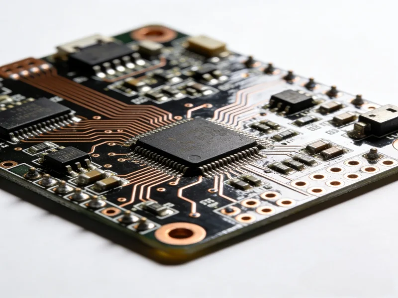
HDI PCBs feature microvias, finer line widths, and multilayer build-up structures that allow for greater component density compared to standard PCBs. These characteristics stem from sequential lamination processes, where additional layers are added to core boards using blind, buried, and through vias. In automotive contexts, HDI PCB automotive applications address the need for miniaturization in engine control units (ECUs), infotainment systems, and power distribution modules. The technology supports high-speed data transmission required for real-time processing, reducing signal loss over short distances. Without HDI, fitting advanced electronics into tight spaces like radar modules or camera assemblies would be impractical. IPC-2226 provides guidelines for designing these interconnects, ensuring they meet density and performance criteria.
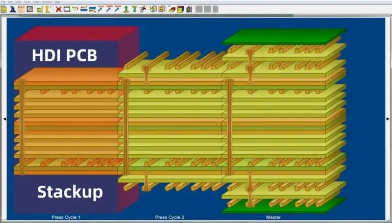
Automotive electronics demand boards that withstand harsh conditions, and HDI PCBs excel by incorporating robust materials and via configurations. Engineers must consider via-in-pad designs and laser-drilled microvias smaller than 150 microns to optimize routing. This relevance grows with electrification, where battery management systems require dense power and signal layers. HDI enables shorter signal paths, minimizing crosstalk and improving impedance control. Ultimately, these boards bridge the gap between semiconductor complexity and vehicle packaging constraints.
HDI PCB Applications in Automotive Systems
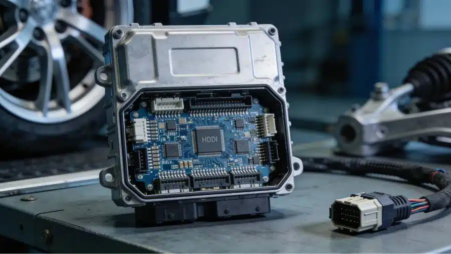
HDI PCB automotive applications span critical areas like powertrain controls, lighting systems, and telematics, where space savings translate to design flexibility. In ECUs, HDI boards integrate multiple microcontrollers and sensors on fewer layers, reducing overall board size by up to 50 percent in compact assemblies. Troubleshooting common issues, such as signal degradation, often involves verifying microvia reliability under load. For infotainment, HDI supports high-resolution displays and connectivity modules with fine-pitch BGAs. These applications highlight HDI's role in balancing density with manufacturability.
Radar and lidar units in safety systems rely on HDI for millimeter-wave signal handling, demanding precise layer stackups. Engineers troubleshoot by simulating RF performance early in design to avoid resonance issues. Power electronics, including inverters, use HDI for gate drivers and IGBTs, where thermal paths integrate directly into the board. This practical approach ensures systems operate seamlessly across vehicle architectures.
HDI PCB in ADAS Systems
HDI PCB ADAS implementations power the core of autonomous driving features, from adaptive cruise control to lane-keeping assistance. These systems process vast data from cameras, ultrasonics, and fusion sensors, requiring HDI for high I/O counts and low-latency interconnects. In central processing units, HDI stackups with Type III or IV configurations handle the density of AI accelerators and GPUs. Troubleshooting focuses on via stub effects that could degrade high-frequency signals above 10 GHz. HDI enables modular ADAS architectures, allowing scalable sensor fusion.
ADAS domain controllers benefit from HDI's ability to embed passives, reducing parasitics in analog front-ends. Practical challenges include aligning microvias with BGA footprints to prevent solder joint failures during vibration. Engineers often iterate stackups to maintain constant dielectric thickness for phase matching. This targeted use of HDI PCB ADAS enhances decision-making speed and accuracy in dynamic environments.
Ensuring HDI PCB Reliability in Automotive Environments
HDI PCB reliability automotive standards demand resilience against thermal cycling, mechanical shock, and humidity, common in under-hood or chassis-mounted units. Microvias are prone to cracking under low-temperature stress, so selecting low-CTE dielectrics prevents delamination. Vibration testing reveals weaknesses in via plating, where barrel cracks propagate from cyclic fatigue. IPC-6012DS outlines qualification for rigid boards in automotive use, emphasizing accelerated life tests. Practical troubleshooting involves X-ray inspection for voiding post-lamination.
Material choices like high-Tg laminates above 170°C ensure stability during reflow and operation. Engineers address reliability by incorporating filled vias to equalize expansion coefficients across layers. Humidity ingress accelerates corrosion in fine features, mitigated by conformal coatings or enclosed housings. These measures extend mean time between failures (MTBF) in field conditions.
Reliability verification includes thermal shock from -40°C to 125°C, simulating real-world exposure. Troubleshooting data logs from strain gauges help correlate failures to CTE mismatches. J-STD-020 guides handling for moisture sensitivity, critical for HDI's thin dielectrics.
HDI PCB Thermal Management in Automotive Applications
HDI PCB thermal management automotive strategies counter heat buildup from power ICs and processors in dense layouts. Microvias concentrate hotspots, so arrays of thermal vias transfer heat to inner planes or external sinks. Engineers calculate junction temperatures using theta-JA models, prioritizing copper pour distribution. High-power ADAS chips exceed 50W, necessitating embedded heat spreaders within the stackup.
Practical solutions include via tents and plugs to block solder wicking while aiding conduction. Troubleshooting overheating involves IR thermography to map gradients post-assembly. Low-loss dielectrics with thermal conductivities above 1 W/mK dissipate RF-generated heat in radar boards. Stackup symmetry prevents warpage under thermal load.
Hybrid approaches combine HDI with metal-core substrates for extreme cases like motor controls. Engineers simulate airflow over fins integrated via cutouts. These techniques maintain delta-T below 20°C for component longevity.
Best Practices for Designing and Manufacturing HDI PCBs for Automotive Use
Start with DFM reviews early, defining aspect ratios below 0.8:1 for microvias to avoid plating voids. Sequential build processes demand precise registration, controlled by fiducials on every layer. For HDI PCB reliability automotive, qualify via chains per IPC-TM-650 methods. Thermal management integrates copper-balanced planes and blind via staggering.
Troubleshooting fabrication issues like laser smear requires plasma desmear optimization. Assembly best practices include low standoff BGAs to minimize shear stress. Simulate power delivery networks to prevent droop in dense HDI fields. Post-process baking per JEDEC standards removes moisture before reflow.
Collaborate on panel utilization to control bow and twist below 0.75%. Field returns often trace to pad cratering, addressed by reinforced via caps.
Conclusion
HDI PCBs drive automotive innovation by enabling compact, high-performance electronics essential for ADAS and beyond. Their applications in ECUs, sensors, and controllers underscore the need for meticulous reliability and thermal strategies. Engineers achieve success through standards-guided design, material selection, and proactive troubleshooting. As vehicles advance toward full autonomy, HDI will remain central, balancing density with durability. Practical implementation ensures these boards meet the rigors of real-world deployment.
FAQs
Q1: What are the key benefits of HDI PCB ADAS systems?
A1: HDI PCB ADAS provides superior signal integrity for high-speed data from sensors, enabling compact modules with more I/O pins. It reduces latency in processing units critical for real-time decisions. Troubleshooting focuses on microvia integrity to avoid failures. Overall, it supports scalable architectures while maintaining automotive-grade reliability.
Q2: How does HDI PCB reliability automotive handle vibration and thermal stress?
A2: HDI PCB reliability automotive uses low-CTE materials and filled vias to withstand vibrations up to 2000 Hz and cycles from -40°C to 125°C. Practical checks include strain analysis during qualification. Robust plating prevents fatigue cracks. This ensures long-term performance in harsh environments.
Q3: What strategies improve HDI PCB thermal management automotive?
A3: HDI PCB thermal management automotive employs thermal via farms, high-conductivity cores, and optimized stackups to dissipate heat from dense components. Engineers use simulations for hotspot prediction. Component placement avoids stacking high-power devices. These practices keep operating temperatures within safe limits.
Q4: Why choose HDI for automotive applications over standard PCBs?
A4: HDI PCB automotive applications offer finer features for miniaturization, fitting advanced electronics in tight spaces like radar housings. It handles high-density routing for mixed-signal designs. Reliability matches standards through build-up processes. Troubleshooting yields fewer interconnect issues compared to through-hole boards.
References
IPC-2226 — Sectional Design Standard for High Density Interconnect (HDI) Printed Boards. IPC.
IPC-6012DS — Qualification and Performance Specification for Rigid Printed Boards in Automotive Applications. IPC.
J-STD-020E — Moisture/Reflow Sensitivity Classification of Nonhermetic Surface Mount Devices. JEDEC.


