Introduction
Buried vias play a critical role in modern multilayer printed circuit board designs, enabling connections between inner layers without penetrating the outer surfaces. These vias support higher routing densities and improved signal performance in high-speed applications. Optimizing buried via size and placement directly impacts manufacturability, reliability, and electrical characteristics. Engineers must balance factors like aspect ratio, plating uniformity, and impedance control to achieve optimal results. This article explores structured approaches to buried via size PCB design and buried via placement guidelines, providing logical engineering insights for effective implementation.
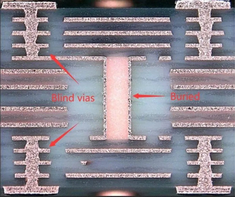
What Are Buried Vias and Why Do They Matter?
Buried vias connect specific inner layers of a multilayer PCB, remaining hidden from the top and bottom surfaces. Unlike through-hole vias, they conserve surface space for components and traces, which proves essential in high-density interconnect boards. This design choice reduces parasitic inductance and capacitance compared to longer vias, enhancing overall board performance. In applications demanding high-speed signals, buried vias minimize path lengths between layers, supporting better signal integrity.
The relevance of buried vias grows with increasing layer counts and data rates in electronics. They enable finer pitch routing and support advanced stackups in telecommunications, computing, and automotive systems. Poor optimization leads to fabrication challenges, such as plating voids or reliability failures under thermal stress. Proper buried via size PCB design ensures compliance with industry expectations for yield and longevity.
Technical Principles Behind Buried Via Performance
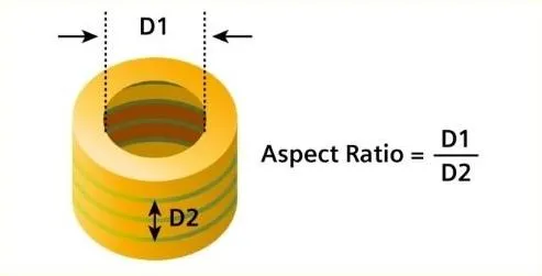
Buried via performance hinges on geometry, material properties, and layer stackup. The via's diameter and depth determine the aspect ratio, which influences copper plating thickness and void formation during fabrication. A higher aspect ratio complicates electrolyte flow, potentially causing incomplete plating and weak barrel strength. Engineers calculate aspect ratio as the ratio of via depth to drill diameter, aiming for values that align with process capabilities.
Signal propagation through buried vias introduces discontinuities that can cause reflections if not managed. The via stub length, though minimal in buried configurations, still affects characteristic impedance, especially at gigahertz frequencies. Smaller diameters reduce inductance but demand precise drilling and etching. Placement relative to traces influences crosstalk, as adjacent vias couple electromagnetically if spaced too closely.
Material selection further modulates these effects. Dielectric constants in core and prepreg layers around the via impact propagation delay. Thermal expansion mismatches between copper and laminate can stress the via under cycling, leading to cracks. IPC-2221 provides foundational guidelines for via dimensions and spacing to mitigate these risks.
Factors Influencing Buried Via Size Selection
Selecting the appropriate buried via size starts with routing density requirements and fabrication limits. Smaller vias maximize board real estate but increase aspect ratio challenges and minimum annular ring constraints. Larger sizes ease manufacturing but occupy more inner layer space, potentially limiting trace escapes. Engineers evaluate trade-offs using stackup simulations to predict drill feasibility across layers.
Annular ring dimensions ensure mechanical robustness around the via pad. Insufficient rings lead to trace breakout during lamination or drilling misalignment. Plating thickness uniformity depends on current density distribution, favoring moderate diameters for even deposition. In buried via size PCB design, consistency across the panel reduces yield variability.
Fabrication processes like sequential lamination define viable size ranges. Laser drilling suits microvias under 100 microns, while mechanical methods handle larger ones. Aspect ratios typically stay below 10:1 for reliability, with lower values preferred for high-current paths to dissipate heat effectively.
Buried Via Placement Guidelines for Optimal Routing
Strategic placement follows buried via placement guidelines to enhance routing efficiency and minimize interference. Position vias near component pads on inner layers to shorten trace lengths, reducing latency in signal paths. Maintain minimum clearances from board edges and other features to avoid drill breakout or stress concentrations. Symmetry in placement across the board aids warpage control during pressing.
For multilayer stackups, align buried vias with layer pairs to simplify sequential build processes. Stagger vias between adjacent layers to prevent alignment errors and overlapping drill zones. Ground plane cuts around vias preserve shielding while allowing access. These practices support higher yields in production.
In dense designs, cluster vias judiciously to group related nets, easing fanout from BGA packages. Avoid placing high-speed signal vias near power planes without adequate spacing to curb noise coupling. Simulation tools verify electromagnetic compatibility before committing to layout.
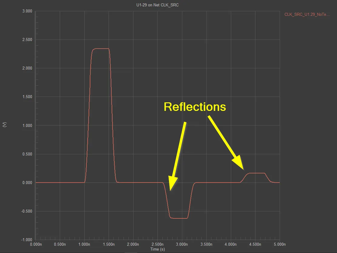
Minimizing Signal Reflections with Buried Vias
Minimizing signal reflections buried via configurations demands precise impedance control throughout the interconnect. Reflections arise from mismatches at via transitions, manifesting as ringing or attenuation in time-domain reflectometry. Buried vias inherently reduce stub lengths, lowering capacitive loading compared to through vias. Pair them with controlled dielectric thicknesses to match trace impedances.
Back-drilling complements buried vias in hybrid designs, removing unused stubs for cleaner transitions. Via diameter selection tunes inductance; finer vias suit high frequencies where wavelength approaches via dimensions. Anti-pad sizing on planes adjusts capacitance, fine-tuning the overall discontinuity.
Differential pairs benefit from paired buried vias with symmetric placement, preserving balance and common-mode rejection. Ground stitching vias nearby absorb return currents, stabilizing reference planes. Pre-layout analysis of S-parameters quantifies improvements, guiding iterations.
IPC-6012 outlines performance specs for via reliability under electrical stress, reinforcing these strategies. Field solvers model TDR responses, confirming reflection coefficients below -20 dB targets.
Best Practices for Implementation
Implement buried via size PCB design by starting with stackup planning. Define layer pairings early to assign buried vias efficiently, minimizing cross-layer jumps. Select drill sizes based on core thicknesses, targeting aspect ratios under 8:1 for standard processes. Verify annular rings meet minimums per class, typically 50 microns finished for inner layers.
Follow buried via placement guidelines with rule decks enforcing spacing: three times drill diameter between vias, five times near edges. Route high-speed nets first, reserving buried vias for critical paths. Incorporate fiducials for registration in sequential builds.
Test prototypes with cross-sections to inspect plating and barrel integrity. Thermal cycling validates reliability per IPC standards. Iterate based on feedback, scaling sizes for production volumes.
- Aspect Ratio: < 10:1 - Plating uniformity
- Via-to-Via Spacing: 3x drill diameter - Crosstalk reduction
- Edge Clearance: 5x drill diameter - Mechanical stability
- Annular Ring: > 50 um - Breakout prevention
Troubleshooting Common Issues
Engineers encounter plating voids when aspect ratios exceed capabilities, addressed by upsizing drills or thinning cores. Misregistration in lamination shifts vias, resolved with tighter tolerances and pilot holes. Signal integrity failures trace to impedance steps, mitigated by tapering anti-pads or adding compensation structures.
Warpage distorts buried vias in asymmetric stackups; balance copper distribution accordingly. High-current heating demands wider barrels, monitored via thermal simulations. Systematic reviews catch these early.
Conclusion
Optimizing buried via size and placement elevates PCB design reliability and performance. Logical adherence to aspect ratios, spacing, and impedance principles yields robust boards. Buried vias excel in high-density, high-speed contexts when engineered thoughtfully. Apply these best practices to streamline workflows and exceed expectations.
FAQs
Q1: What key factors determine buried via size in PCB design?
A1: Buried via size PCB design balances routing density, aspect ratio, and manufacturability. Smaller diameters increase density but raise plating challenges, while larger ones simplify fabrication at the cost of space. Follow stackup-specific limits, typically with aspect ratios below 10:1. Consult process capabilities to ensure annular ring integrity and plating uniformity for reliable performance.
Q2: How do buried via placement guidelines improve signal integrity?
A2: Buried via placement guidelines position vias to shorten paths and maintain plane references, reducing latency and EMI. Space them adequately from edges and each other to prevent coupling. Symmetric layouts aid thermal stability. This approach minimizes discontinuities, supporting high-speed operations effectively.
Q3: Why focus on minimizing signal reflections with buried via strategies?
A3: Minimizing signal reflections with buried via methods controls impedance mismatches and stub effects. Shorter buried paths lower inductance, paired with precise anti-pad sizing. Ground stitching enhances return paths. Simulations verify low reflection coefficients, ensuring clean eye diagrams at multi-GHz rates.
Q4: What role do standards play in buried via optimization?
A4: Standards like IPC-2221 and IPC-6012 guide buried via dimensions, spacing, and qualification. They specify annular rings and reliability tests, preventing common failures. Consistent application boosts yield and interoperability across fabricators.
References
IPC-2221B - Generic Standard on Printed Board Design. IPC, 2003
IPC-6012E - Qualification and Performance Specification for Rigid Printed Boards. IPC, 2017
IPC-2226 - Design Standard for High Density Interconnect (HDI) Printed Boards. IPC, 2002


