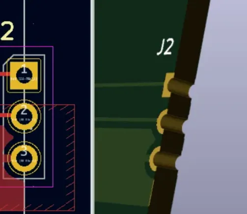
A board that looks perfect in KiCad can still be rejected by the fabricator or suffer yield loss on the production line. The usual reason is simple: the design rules used during layout do not match the manufacturer's actual process capabilities. Traces are too narrow, clearances are insufficient, vias fall below minimum annular ring, or footprints contain features the fab cannot reliably produce.
This article focuses on the critical transition from design to manufacturing. It explains the real constraints used by PCB factories, how to configure KiCad design rules to match those constraints, the most common issues that trigger DFM rejects, and practical engineering recommendations that reduce risk before you generate Gerbers. The goal is to help you deliver boards that pass both local DRC and the manufacturer's engineering review on the first submission.
Understanding Manufacturing Constraints in KiCad
PCB factories operate within physical process limits. These limits are not theoretical—they are determined by etching tolerance, drilling accuracy, plating capability, and solder-mask registration. Designing outside them creates scrap, extra charges, or delayed deliveries.
Trace Width
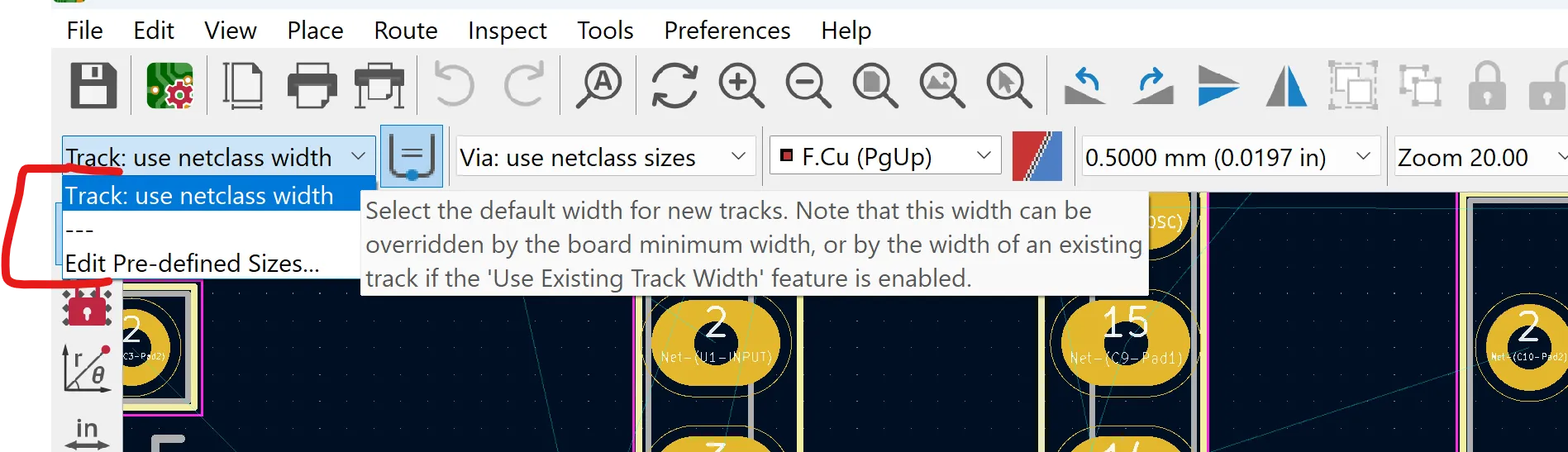
Minimum trace width is set by the copper weight and the etching process. Most standard processes support 0.10–0.15 mm (4–6 mil) for outer layers. Narrower traces increase the risk of open circuits or etching undercut. High-current traces must be calculated for temperature rise, not just the minimum rule.
Clearance
Clearance (copper-to-copper spacing) must account for etching tolerance and solder-mask dam requirements. A common production minimum is 0.10–0.15 mm. Clearances tighter than the fab's capability produce shorts or require more expensive processes.
Via Size
Via drill size and annular ring are limited by drilling accuracy and plating thickness. A typical reliable combination is 0.20–0.30 mm drill with at least 0.125 mm annular ring. Smaller vias raise cost and reduce yield.
Hole Size
Finished hole size after plating must meet the component lead or press-fit requirement. The designer must allow for plating thickness when specifying the drill size. Unsupported hole sizes or aspect ratios (board thickness ÷ hole diameter) that exceed the fab's limit cause plating voids.
Manufacturing perspective: every rule you set in KiCad should be equal to or more conservative than the target factory's published capabilities. Rules that are tighter than the process can deliver will be flagged during DFM review.
How to Configure KiCad Design Rules for PCB Manufacturing
Board Setup
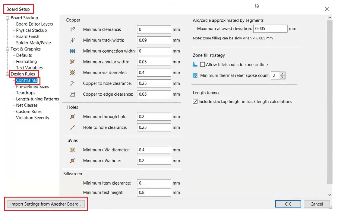
Open Board Setup → Design Rules. Start by selecting or creating a constraint set that reflects the manufacturer you intend to use. Enter the minimum track width, clearance, via diameter, and annular ring values taken from the fab's capability document—not from KiCad's default template.
Net Classes
Create separate net classes for power, ground, high-speed signals, and general routing. Assign appropriate track widths and clearances to each class. Power nets typically need wider traces; sensitive signals may need controlled impedance rules. The interactive router and DRC will then enforce these values automatically.
Clearance Rules
In the custom design rules editor you can set clearance between specific net classes or between copper and board edge. Always include a copper-to-edge clearance (usually 0.3–0.5 mm) to satisfy most manufacturers' requirements. Save the rule set with the project so every collaborator works to the same manufacturing limits.
Practical guidance: load the manufacturer's rules at the beginning of the layout, not at the end. Changing rules after routing is complete forces extensive rework.
Common KiCad Design Issues That Affect Manufacturing
Too Narrow Traces
Designers sometimes use the absolute minimum width for every net. High-current paths then overheat, and etching tolerance can break narrow traces. Calculate current-carrying capacity and apply wider traces where needed.
Insufficient Spacing
Clearances copied from a previous project or left at default values frequently fall below the fab's limit. This is one of the top reasons for DFM rejection.
Incorrect Footprints
Pads that are too small, missing thermal reliefs, or have non-standard shapes create soldering defects. Always verify footprints against both the component datasheet and the manufacturer's land-pattern guidelines.
Unsupported Features
Via-in-pad without filling, extremely small microvias, non-standard aspect ratios, or copper features closer than the minimum solder-mask dam are often unsupported on standard processes. Confirm capability before using them.
These issues are rarely caught by a DRC that uses optimistic rules. They appear only when the manufacturer runs its own engineering review.
KiCad DRC Check Before Manufacturing
What DRC Detects
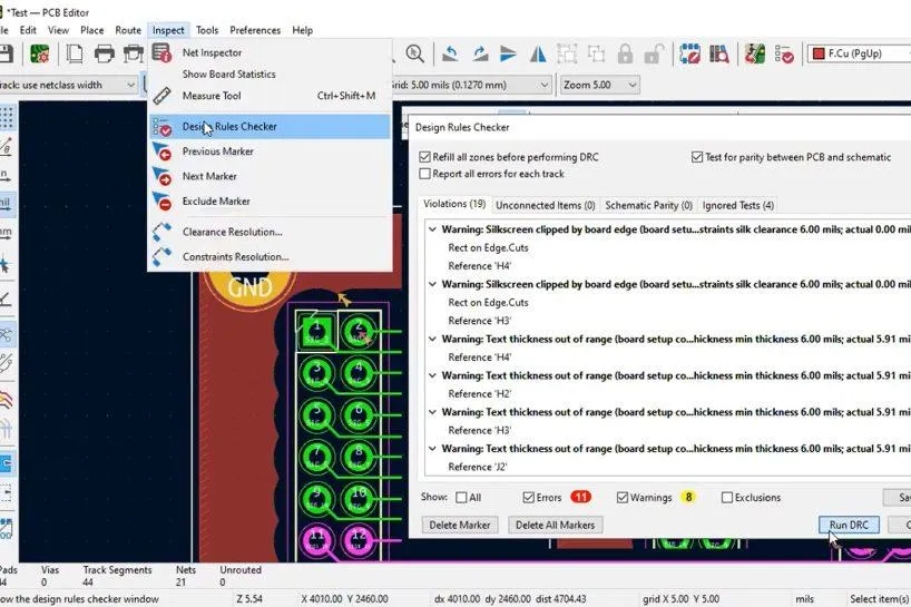
With manufacturing-aware rules loaded, DRC reports track-width violations, clearance errors, via annular-ring problems, hole-to-hole spacing issues, copper-to-edge violations, and silkscreen conflicts. It is the last automated filter before Gerber generation.
How to Fix Common Errors
- Track too narrow → increase width or move the net to a wider net class.
- Clearance violation → adjust routing or relax the rule only if the fab confirms it is acceptable.
- Annular ring too small → enlarge the via pad or reduce the drill size within capability limits.
- Copper too close to edge → pull copper inward or enlarge the board outline keep-out.
Run DRC after major routing sessions and once more immediately before exporting manufacturing files. A clean result against realistic rules is the strongest indicator that the board will pass the factory's DFM check.
AIVON Engineering Recommendations for KiCad Users
From the manufacturing side, the most effective optimization is to design inside the process window from the first day of layout.
- Load the target factory's minimum trace, clearance, via, and hole values into KiCad before placement begins.
- Keep copper distribution reasonably balanced between layers to reduce warpage risk.
- Use standard via sizes and avoid exotic features unless the project truly requires them.
- Generate a complete package—Gerbers, drill files, BOM, and pick-and-place—then verify it in a Gerber viewer.
- When the design is ready, the AIVON KiCad plugin allows engineers to move directly from the verified board into quotation and ordering while preserving the exact design data. This eliminates manual file re-packaging errors and gives the engineering team an immediate DFM perspective.
Designing with real factory constraints, running a manufacturing-aware DRC, and delivering a clean file set is the practical difference between boards that need respins and boards that go straight into production.
Preparing KiCad design rules for manufacturing is not an extra step at the end of the project—it is the framework that should guide every layout decision. When the rules match the factory's process, the board that leaves your computer is the board that can be built reliably and cost-effectively.
FAQ
Q1: What design rules should I set in KiCad for PCB manufacturing?
A1: Set minimum track width, clearance, via drill size, annular ring, and copper-to-edge clearance according to your manufacturer's published capabilities. Create net classes so power and signal nets receive appropriate values automatically.
Q2: Why does my KiCad board pass DRC but still get rejected by the manufacturer?
A2: Local DRC only checks the rules you loaded. If those rules are more aggressive than the fab's process limits, the manufacturer's DFM review will flag the violations. Always configure rules to the actual factory capabilities.
Q3: How do I avoid traces that are too narrow for manufacturing in KiCad?
A3: Calculate current requirements for power nets and assign them to wider net classes. For signal nets, use the manufacturer's standard minimum rather than the absolute smallest value the tool allows.
Q4: What is the most common KiCad design issue that causes manufacturing problems?
A4: Insufficient clearance and incorrect footprints are among the top causes. Both are prevented by loading realistic design rules early and verifying every footprint against the datasheet and fab guidelines.
Q5: When should I run the KiCad DRC before sending files to manufacturing?
A5: Run DRC after placement, after major routing, and once more immediately before generating Gerbers. A final clean result against manufacturing-aware rules significantly reduces the chance of DFM rejection.
```