Introduction
High-speed digital designs push the boundaries of performance in modern electronics, relying heavily on multilayer printed circuit boards to manage complex signal paths and power delivery. As data rates climb into gigabits per second, engineers face intensified challenges in maintaining signal quality across multiple layers. Multilayer PCBs offer the density and controlled environments needed for such applications, but they introduce issues like crosstalk, reflections, and noise coupling. Key concerns include signal integrity in digital circuits, precise impedance control for high-speed traces, robust power distribution network design, and strategies for reducing EMI in digital PCBs. Addressing these requires a deep understanding of high-speed PCB design rules to ensure reliable operation. This article explores these challenges and provides structured solutions for electric engineers.
Why Multilayer PCBs Are Essential for High-Speed Digital Design
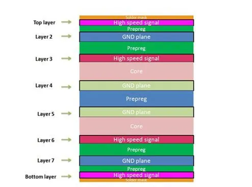
Multilayer PCBs enable the separation of signal, power, and ground planes, which is critical for isolating high-speed signals from noise sources. In single or double-layer boards, signals share spaces with power lines, leading to excessive interference and degraded performance. With 8 to 16 layers or more, designers can dedicate inner layers to ground and power, creating return paths that minimize loop inductance. This stackup strategy directly supports signal integrity in digital circuits by reducing common-mode noise and improving shielding. Industry relevance grows with applications in telecommunications, computing, and automotive systems, where failure to manage these aspects results in bit errors or system crashes. Adopting multilayer constructions aligns with the demands of rising edge speeds and frequencies.
Core Challenges in Signal Integrity for Digital Circuits
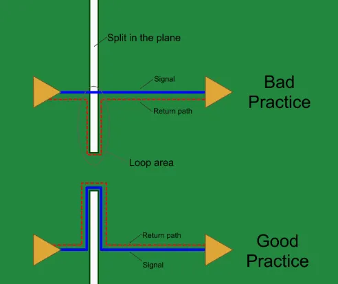
Signal integrity in digital circuits refers to preserving the electrical quality of signals from transmitter to receiver, preventing distortion that causes timing errors or data corruption. In multilayer PCBs, primary issues arise from reflections due to impedance mismatches, crosstalk between adjacent traces, and ground bounce from simultaneous switching. At high speeds, signals behave more like transmission lines, where even small discontinuities like vias or bends introduce losses. Dielectric variations across layers exacerbate attenuation, especially in thicker stacks. Engineers must analyze eye diagrams and insertion loss to quantify these effects early in the design cycle. Proper high-speed PCB design rules mitigate these by enforcing length matching and via optimization.
Achieving Impedance Control for High-Speed Traces
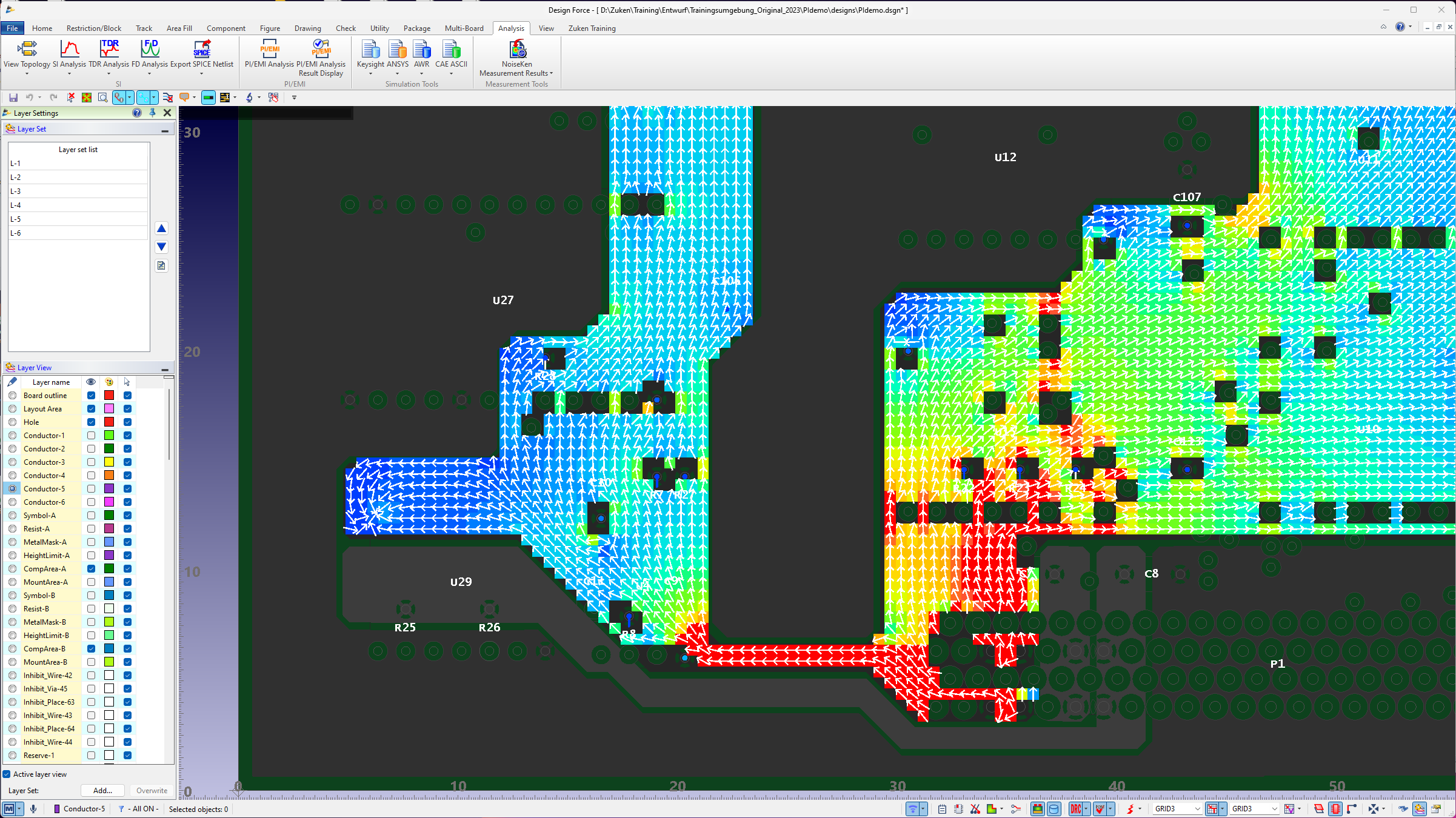
Impedance control for high-speed traces ensures characteristic impedance remains consistent along the signal path, typically 50 ohms single-ended or 100 ohms differential. In multilayer boards, this involves precise control of trace width, thickness, dielectric height, and material properties like dielectric constant. Variations in copper plating or glass weave skew can cause tolerance deviations exceeding 10 percent, leading to reflections. Stackup planning positions signals between reference planes to leverage microstrip or stripline configurations, each with distinct field distributions. IPC-2141 provides guidelines for calculating and verifying controlled impedance, emphasizing fab process capabilities. Testing with time-domain reflectometry confirms compliance before assembly.
Designing Effective Power Distribution Networks
Power distribution network design in multilayer PCBs focuses on delivering stable voltage with minimal ripple and impedance to active components. Decoupling capacitors placed near ICs form local reservoirs, but the plane structure provides the low-inductance path for high-frequency currents. Splitting planes creates isolated domains for different voltage rails, preventing noise coupling between them. Vias stitching ground and power planes reduce slot resonances that act as antennas. High-speed PCB design rules dictate plane thickness and via density to achieve target impedance profiles below milliohms at operating frequencies. Simulations reveal PDN resonances, guiding adjustments for uniform current spreading.
Strategies for Reducing EMI in Digital PCBs
Reducing EMI in digital PCBs involves containing radiated and conducted emissions from fast-switching signals. Clock lines and data buses generate harmonic-rich spectra that couple through board edges or cables if not shielded. Solid ground planes act as shields, with closely spaced power-ground pairs forming stripline-like transmission lines for signals. Guard traces or moats isolate sensitive analog sections from digital noise. IPC-2251 outlines practices for high-speed packaging to minimize electromagnetic interference through layout and partitioning. Compliance testing verifies field strengths stay within limits, often requiring iterative shielding additions.
High-Speed PCB Design Rules: Layer Stackup and Routing Best Practices
High-speed PCB design rules start with stackup definition, balancing symmetry for warpage control and routing channels for density. Core and prepreg selection influences dielectric losses, favoring low-loss materials for outer layers. Routing mandates length-matched pairs for differential signals, avoiding 90-degree bends in favor of 45-degree or curved paths to reduce reflections. Via transitions demand back-drilling or blind vias to eliminate stubs longer than a fraction of the wavelength. IPC-2221 establishes generic requirements for conductor spacing and plane clearances, supporting overall integrity. Pre-layout simulations validate rules before committing to fabrication.
Practical implementation includes grouping high-speed signals on inner layers adjacent to planes, minimizing via count through fanout optimization. Differential pairs require symmetric routing with controlled spacing for odd-mode impedance. Power planes feature cutouts only where necessary, with overlapping minimized to avoid capacitance. These rules ensure signal integrity in digital circuits across the board.
Via Design and Transition Management
Vias pose significant discontinuities in high-speed paths due to their parasitic inductance and capacitance. Through-hole vias create stubs that reflect at frequencies where stub length equals quarter-wavelength. Back-drilling removes unused portions, while blind or buried vias confine transitions to specific layers. High-speed PCB design rules specify via diameter relative to trace width, often 50 percent or less, with anti-pad sizing per plane clearance needs. Multiple vias in parallel reduce effective inductance for return currents. Ground via fences around signal vias improve shielding and return path integrity.
Material Selection and Fabrication Considerations
Material selection impacts loss tangent and propagation delay uniformity, crucial for impedance control for high-speed signals. Low-Dk/Df laminates reduce attenuation, but cost and availability guide choices. Fabrication tolerances for dielectric thickness directly affect impedance, requiring tight specs like plus or minus 10 percent. Sequential lamination builds complex stacks without stressing inner layers. Adhering to high-speed PCB design rules during fab handover prevents yield issues from asymmetric builds.
Troubleshooting Common High-Speed Issues
Engineers often encounter eye closure from crosstalk, addressed by increasing spacing or adding shielding planes. PDN droop under load points to insufficient decoupling, resolved by adding mid-layer caps or thickening planes. EMI spikes trace to unshielded edges, fixed with perimeter stitching vias. Iterative simulation and prototype testing refine designs. These insights stem from systematic application of high-speed PCB design rules.
Conclusion
Overcoming challenges in high-speed digital design with multilayer PCBs demands rigorous adherence to signal integrity in digital circuits, impedance control for high-speed traces, power distribution network design, and reducing EMI in digital PCBs. Structured stackups, precise routing, and validated rules form the foundation for success. By integrating these practices, engineers achieve reliable performance at multi-gigabit speeds. Future designs will leverage even denser layers, but core principles remain timeless. Prioritizing these elements ensures robust, compliant boards ready for demanding applications.
FAQs
Q1: What are the key high-speed PCB design rules for maintaining signal integrity in digital circuits?
A1: High-speed PCB design rules emphasize controlled impedance traces, length matching for clocks and data, and adjacent reference planes to minimize loop areas. Vias should use back-drilling to eliminate stubs, and routing avoids sharp bends. Decoupling capacitors near ICs stabilize supply noise. These practices prevent reflections and crosstalk, ensuring clean eye patterns. Simulations verify compliance before fab.
Q2: How does impedance control for high-speed signals impact multilayer PCB performance?
A2: Impedance control for high-speed signals prevents reflections by matching trace geometry to target values like 100 ohms differential. In multilayer stacks, dielectric spacing and plane proximity dictate microstrip or stripline choices. Tolerances below 10 percent require precise fab specs. Poor control degrades signal integrity in digital circuits, causing jitter. Verification via TDR testing confirms design goals.
Q3: Why is power distribution network design critical in high-speed multilayer PCBs?
A3: Power distribution network design provides low-impedance paths for transient currents, preventing voltage droop during switching. Planes with stitching vias distribute current evenly, while split domains isolate rails. High-speed PCB design rules guide capacitor placement for broadband decoupling. Weak PDN leads to ground bounce and EMI. Simulations target impedance curves for optimal stability.
Q4: What techniques are effective for reducing EMI in digital PCBs?
A4: Reducing EMI in digital PCBs involves solid ground planes, minimal loop areas, and shielding for clocks. Guard traces isolate sections, and edge stitching contains fields. Proper PDN lowers simultaneous switching noise. These align with high-speed PCB design rules for partitioning. Pre-compliance scans guide refinements for regulatory pass.
References
IPC-2221C — Generic Standard on Printed Board Design. IPC, 2023
IPC-2141A — Design Guide for High-Speed Controlled Impedance Circuit Boards. IPC, 2004
IPC-2251 — Design Guide for the Packaging of High Speed Electronic Circuits. IPC, 1999


