


Engineering Cases
Engineering Cases focuses on real PCB engineering reviews, manufacturing challenges, and production optimization processes from actual fabrication projects. This category highlights how different PCB designs are evaluated and adjusted during engineering review, covering topics such as stack-up analysis, impedance control, drill optimization, copper balancing, solder mask alignment, DFM review, and production risk assessment across various PCB applications. The content in this section is based on practical manufacturing scenarios rather than theoretical introductions. Each engineering case demonstrates how specific PCB issues are identified, analyzed, and resolved during production preparation and fabrication. These records help engineers, purchasers, and hardware teams better understand the relationship between PCB design decisions and manufacturing stability, yield control, and process reliability. Topics may include multilayer PCB engineering review, HDI process optimization, flexible PCB manufacturing considerations, heavy copper processing adjustments, surface finish selection, Gerber data verification, and other real-world PCB production experiences. By organizing engineering challenges and process solutions into structured case content, this category provides valuable insight into practical PCB manufacturing and engineering workflow management.
Featured Blog
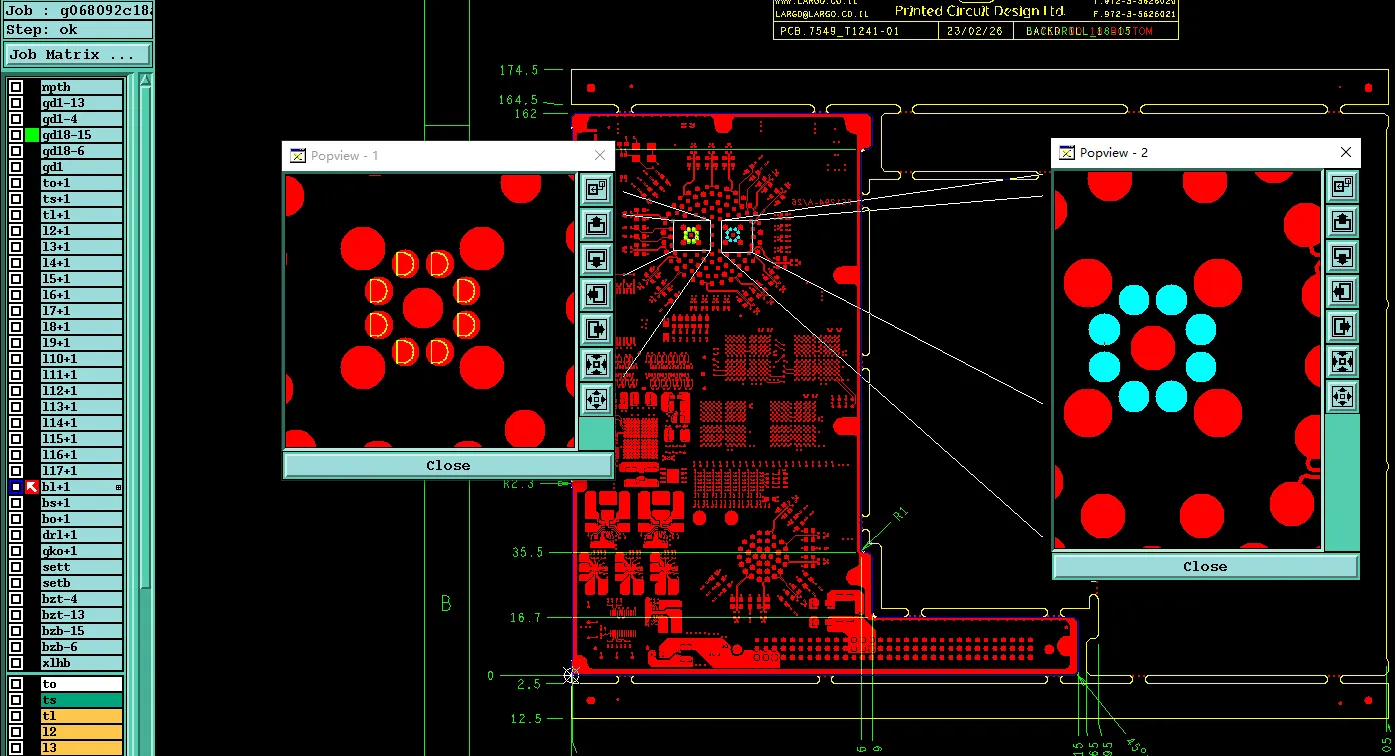
PCB Hole Attributes and Special Drilling: Common CAM Review Conflicts
See how CAM reads PCB hole attributes and special drilling—PTH vs NPTH, back drill, press-fit holes, countersink, and laser vias—and why incomplete data delays fabrication.
Latest Blogs
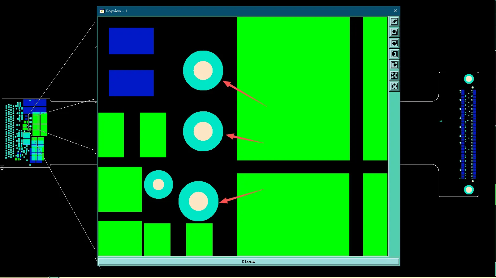
How CAM Review Fixed Stackup, Via Tenting & Outgassing Conflicts on a 7-Layer Rigid-Flex PCB
Real CAM engineering review of a 7-layer rigid-flex PCB. Learn how stackup substitution, via tenting conflicts, PI stiffener gaps and solder mask outgassing risks were resolved to avoid delamination, yield loss and production delays.
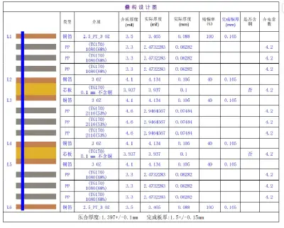
How a 0.1 mm Stackup Mismatch and Material Shortage Halted a 6-Layer 3 oz PCB Order
Discover key DFM lessons on 6-layer PCB stackups. Learn how to handle 3 oz heavy copper thickness errors and TG170 to NP-175FTL material substitutions in CAM.
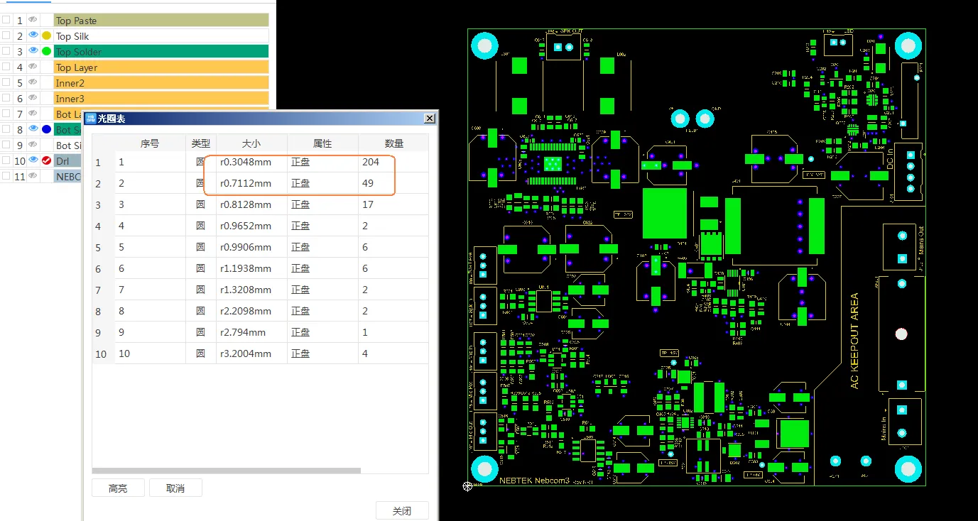
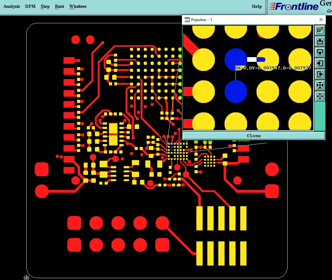
How DFM Prevented Via Tenting Issues in 4-Layer FR4 PCB
Learn how DFM review resolved via tenting mismatches, stackup conflicts, and undersized silkscreen in a 4-layer FR4 PCB, preventing yield loss, solder wicking, warpage, and reliability risks before production.
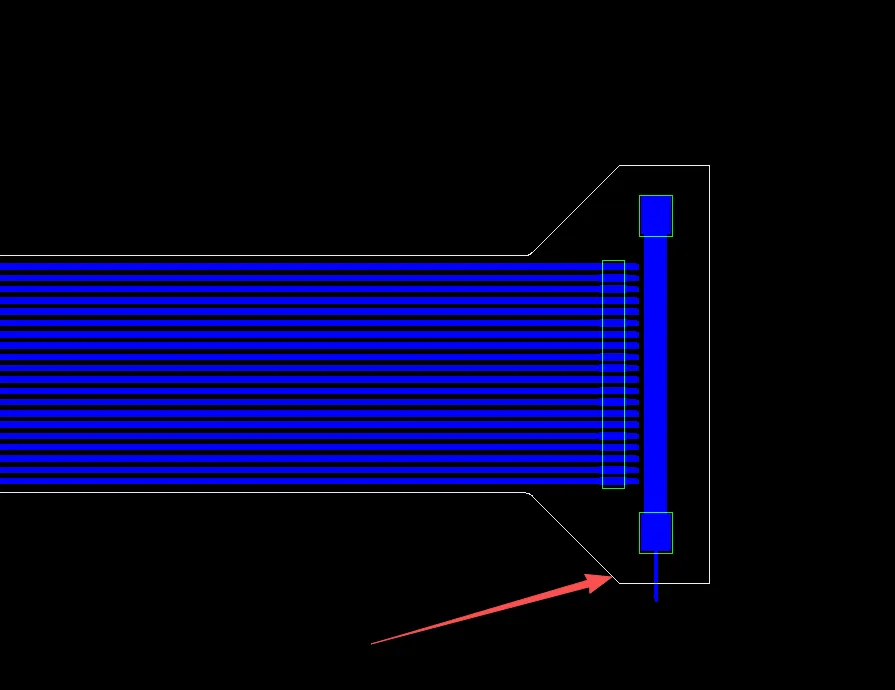
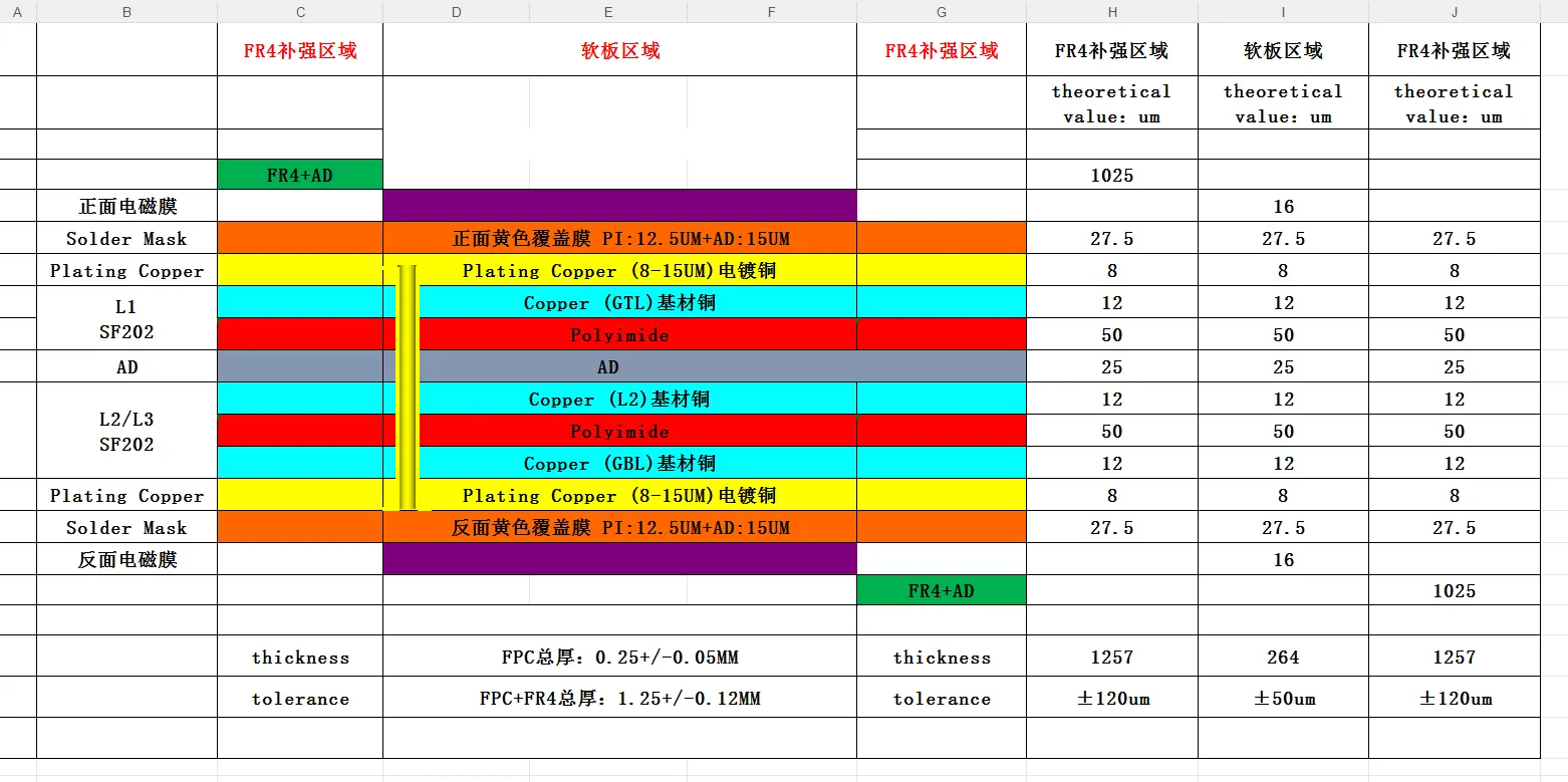
Can 0.1mm PI Stiffener Achieve 0.3mm FPC Total Thickness?
See how a 0.1 mm PI stiffener could not reach the requested 0.30 mm total thickness on a long single-layer FPC—and the zone-specific tolerances plus hard-gold lead fix that kept the process stable.
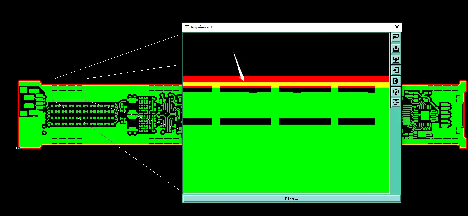
Preventing Exposed Copper from Copper to Outline Clearance Issues
Learn how DFM review fixed tight copper to outline clearance on a 6-layer FR4 PCB to prevent exposed copper after routing. Key steps: 8 mil copper shave, process edge tooling marks, and original solder mask openings for better yield and reliability.
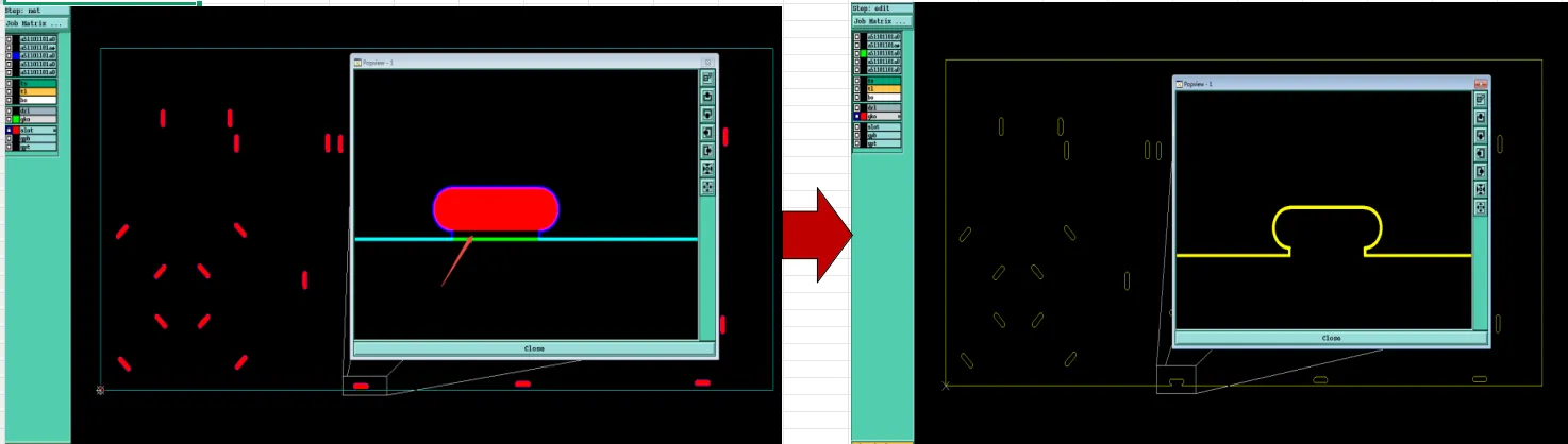
1-Layer PCB DFM Guide: Handling Empty Layers & Slot Clearance
Avoid CAM review holds on single-sided PCBs. Learn how to handle empty Gerber layers, slot clearance issues, and missing drawing text during PCB CAM review.
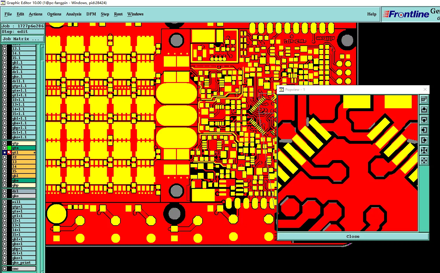
How DFM Prevented Heavy Copper Etch Failures in Multilayer PCB
This case applies Heavy Copper PCB Design Rules to show how DFM review fixed tight clearances with pad shaving, limited resin fill to 0.3 mm vias, and approved stackup substitution, preventing residual copper bridges, via voids, and material lead-time delays.
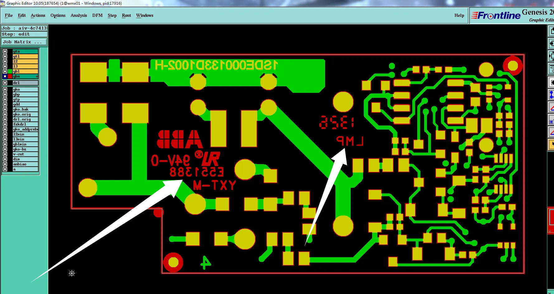
How We Resolved Serial ID Marking on 4-Layer ENIG PCB
CAM review of a small 4-layer ENIG board found no silkscreen layer and insufficient solder-mask space for required sequential IDs and UL marks. Marks were relocated to clear top-side areas to meet IPC-4552 without reducing clearance.
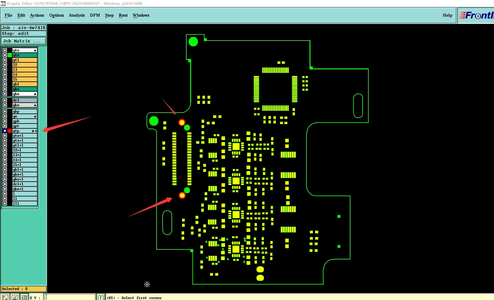
How DFM Handled Undersized Silkscreen on Dense 6L PCB
This case shows how DFM review handled Silkscreen Minimum Size limits on a dense 6-layer FR-4 board where characters fell below 0.1 mm width and 0.7 mm height, confirming possible blur and fixing paste-to-mask opening mismatches for reliable production.
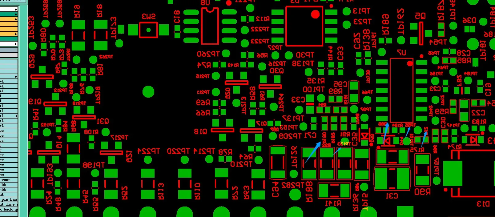
Preparing Customer Self-Panel Layout for 4-Layer PCB Production
Learn how engineers prepared a high-volume 4-layer PCB by confirming the 1x3 customer self-panel layout from the single-board file, accepting silkscreen characters below process limits, and adding UL certification plus date code for full traceability and efficient production.
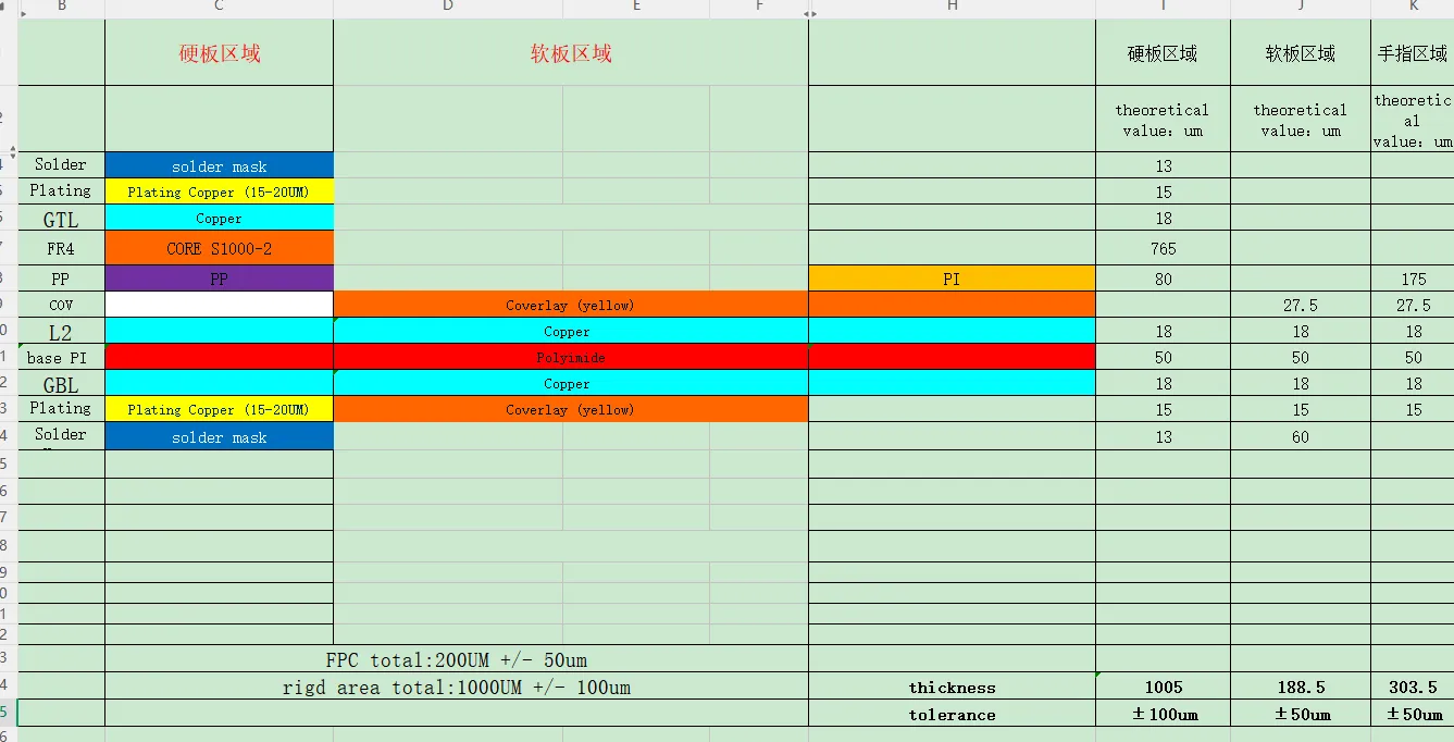
Rigid-Flex PCB Stackup Design: Balancing for Warpage Control
Engineering evaluation of asymmetrical rigid-flex PCB stackup design challenges. Discover how process controls manage warpage, thickness tolerances, and PI stiffener reliability for consistent, manufacturable hybrid boards.
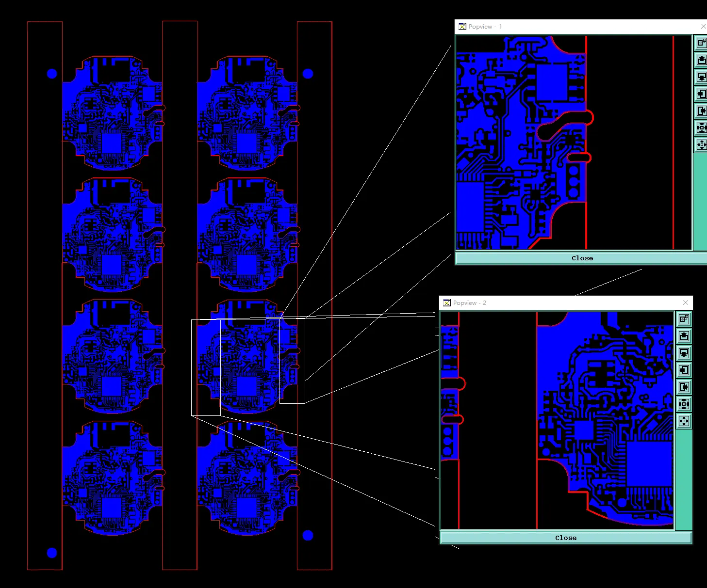
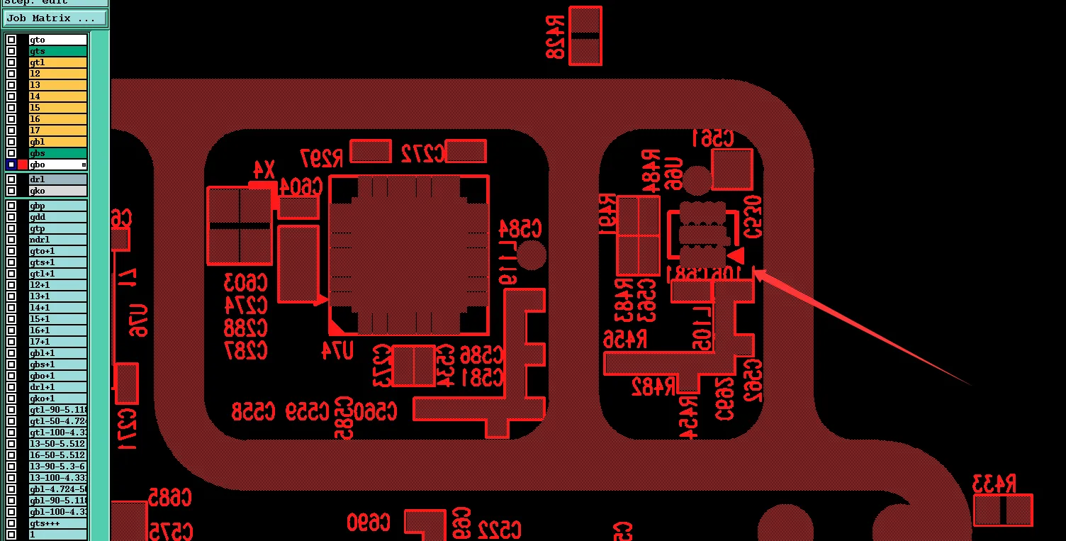
Trace to Board Edge Clearance: Essential DFM Rules
DFM review prevented copper exposure and yield loss by correcting insufficient trace-to-board-edge clearance on a 4-layer FR4 PCB with V-cut and routing separation, plus silkscreen-on-pad risks.


