In PCB manufacturing, aluminum-based boards with heavy copper present unique production hurdles that standard FR4 designs rarely encounter. This case examines a real 2-layer aluminum PCB order (91 × 70 mm, 2.0 mm thick, 3oz outer copper) where multiple manufacturability issues surfaced during CAM engineering review. Our team identified risks related to thick copper processing, via plugging, hole metallization, solder mask application, and legend printing. These issues required direct customer confirmation to avoid defects ranging from delamination to short circuits.
Heavy copper aluminum PCBs are popular for thermal management in power electronics and LED applications, yet the combination of 3oz copper foil height and aluminum substrate significantly narrows the process window. This article details the engineering questions (EQs) raised, the reasoning behind each, potential failure modes if ignored, and how the issues were resolved. It highlights why thorough CAM review remains essential before releasing such boards to production.
Order Overview
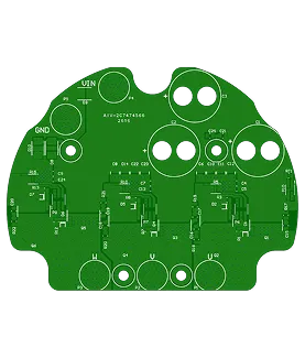
The order specified a 2-layer aluminum base PCB ( #ALU-20260511-016 ) using TG130 material, 2.0 mm finished thickness, and asymmetric copper weights with 3oz on the outer layers. Surface finish was ENIG, with a minimum hole size of 0.2 mm. The design included resin-plugged vias, mechanical forming, and 100% AOI testing. Panelization was 1×1 single pieces, quantity 10 pcs (10 sets). Delivery was set at 22 days with Aivon as supplier.
Key characteristics included aluminum substrate for heat dissipation (3.0 W/m·K thermal conductivity), no V-cut, and specific requirements for solder mask (green) and legend (white). The board also featured larger holes at 3.2 mm and 6.0 mm. These parameters immediately flagged the need for careful stackup validation and process adjustments typical for thick-copper aluminum constructions.
Main Engineering Questions Found During CAM Review
Copper Clearance Adjustment to Prevent Drilling Shorts
We noticed that certain copper features were positioned too close to drill locations on this 3oz aluminum board. Our CAM engineer recommended removing 0.3 mm of copper on one side around critical holes. This adjustment was necessary because thick copper foil can lift or burr during drilling, especially on aluminum substrates where thermal expansion differs from copper.
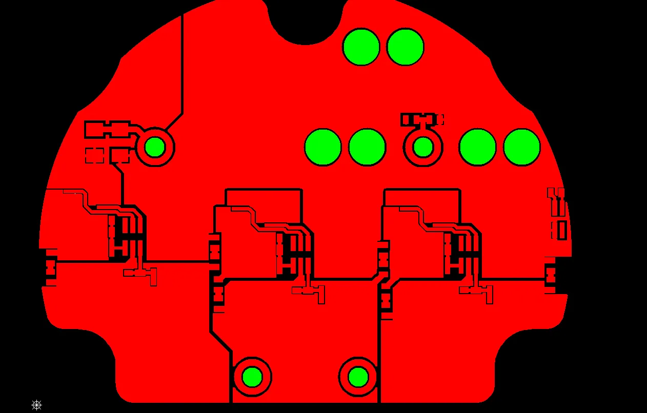
Figure 1: removing 0.3 mm of copper on one side around critical holes
If ignored, exposed or lifted copper edges could cause short circuits after depanelization or during assembly. In extreme cases, this leads to intermittent electrical failures or complete board scrap. According to typical IPC-A-600 acceptability criteria, such edge defects increase reliability risks in high-current applications where this board would be used.
Solder Mask Process Adaptation for 3oz Copper
Because the board uses 3oz copper, standard single-pass solder mask printing would not achieve adequate coverage on the high copper steps. Our engineer confirmed the need for a double-printing process: first with transparent ink for better filling, followed by the specified green ink. This is a common adaptation for heavy copper boards to ensure proper mask thickness and adhesion.
Without this confirmation and process change, thin mask areas over copper traces could result in poor insulation, solder bridging during assembly, or exposed copper prone to oxidation. We have seen such cases lead to assembly failures and costly field returns when the initial mask coverage proves insufficient.
Silkscreen Legibility on Thick Copper
We identified multiple character locations where the 3oz copper height made it difficult for ink to adhere properly. Similar positions could not be enlarged without violating design constraints. The finished boards would need customer acceptance of potentially blurry or incomplete legend markings on the substrate areas.
If unaddressed, this could cause assembly confusion or quality inspection failures. While cosmetic, unclear legends sometimes mask underlying process issues and complicate traceability. Our team has observed that designers frequently underestimate how copper height affects legend quality on heavy copper boards.
Large Hole Metallization Change (PTH to NPTH)
The 3.2 mm and 6.0 mm holes could not reliably plate through the aluminum substrate using standard PTH processes. Our production team proposed treating these as NPTH (non-plated) holes. This decision stems from the physical limitation of aluminum material preventing proper plating in larger diameters without specialized (and costly) processing.

Figure 2: treating 3.2 mm and 6.0 mm holes as NPTH holes
Ignoring this would risk incomplete plating, voids, or unreliable electrical connectivity if PTH was forced. In production, this often results in open circuits or mechanical weakness at mounting points.
Stackup and Insulation Layer Modification
Due to the 3oz copper, the original 50 μm insulation layer specification was unfeasible. Our engineering review revealed that such a thin dielectric would create high risk of delamination under thermal stress. We proposed an adjusted stackup structure to maintain reliable bonding between copper and aluminum core.
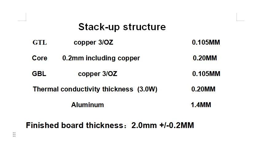
Figure 3: adjusted stackup structure
Proceeding without this change could cause layer separation during reflow soldering or field operation, leading to complete board failure, warpage, or copper peeling. This is particularly critical for aluminum PCBs where thermal cycling is common.
Manufacturing Risks and DFM Insights
This case underscores several recurring DFM pitfalls with heavy copper aluminum boards. Designers often specify tight insulation layers without considering actual copper foil thickness effects on lamination pressure and resin flow. The 3oz copper creates pronounced topography that challenges both solder mask and legend processes.
Another common mistake is assuming all holes can be plated through regardless of substrate material and diameter. Aluminum introduces additional constraints compared to FR4. If EQs are ignored, consequences include resin voids, copper lift, poor solderability, via cracking under thermal stress, and reduced overall yield. Production delays from rework or scrap multiply costs quickly.
Our CAM workflow caught these before panel production, preventing potential batch failure. Early clarification also avoids multiple revision cycles that frustrate both sides.
How the Engineering Team Resolved the Issues
After internal review, we compiled a clear EQ list with proposed modifications, including visual references for the adjusted stackup and copper clearances. The customer confirmed acceptance of the double solder mask process, NPTH treatment for large holes, and legend quality expectations. Stackup was revised to a manufacturable dielectric thickness while preserving thermal performance.
Our team performed final CAM output validation, confirming no remaining conflicts in drill files, solder mask openings, or outline data. These steps protected yield and ensured the boards met functional requirements for the intended application.
Final Manufacturing Outcome
All engineering questions were resolved through customer confirmation. Production files were updated accordingly, and the order was released for fabrication. The adjusted parameters aligned with standard aluminum heavy copper manufacturing capabilities, minimizing risks during lamination, drilling, plating, and surface finishing stages.
Key Takeaways for PCB Designers
- Provide complete stackup details including dielectric thickness expectations when using copper weights above 2oz. Early discussion prevents last-minute adjustments.
- Account for copper foil height when defining solder mask and legend requirements. Consider double printing or adjusted clearances for 3oz+ designs.
- Clearly specify hole plating intent (PTH/NPTH) especially for larger diameters on metal-core boards. Not all holes are suitable for plating.
- Include adequate copper clearance around drill locations in heavy copper designs to accommodate potential foil movement.
- Use consistent fabrication notes and avoid conflicting requirements between layers or drawings.
- Prepare for potential legend quality trade-offs on thick copper boards and communicate acceptance criteria upfront.
- Request DFM review early in the design phase for aluminum or heavy copper projects to reduce EQ volume and lead time.
FAQ
Q1: Why is copper clearance adjustment necessary around drill holes on thick copper aluminum PCBs?
A1: Thick copper foil (3oz) can shift or lift slightly during mechanical drilling, especially on aluminum substrates with different expansion rates. The 0.3 mm clearance prevents short circuits from burrs or lifted copper contacting hole walls.
Q2: Can 3oz copper boards use standard single-pass solder mask printing?
A2: Usually not. The high copper topography requires double printing (transparent base + final color) for adequate coverage and to avoid thin spots that cause solder bridging or reliability issues.
Q3: Why do large holes on aluminum PCBs often need to be NPTH instead of PTH?
A3: Aluminum material complicates reliable through-hole plating for larger diameters (3.2 mm+). Forcing PTH can cause plating voids or poor adhesion. NPTH is safer and more reliable for mechanical mounting holes.
Q4: What causes delamination risk when using thin insulation layers with 3oz copper?
A4: Thick copper requires higher lamination pressure and temperature. A 50 μm dielectric is often insufficient to flow properly and bond reliably, leading to voids or separation under thermal stress. Adjusted thicker dielectrics mitigate this per common material guidelines.
Q5: How should designers prepare legend data for heavy copper boards?
A5: Expect reduced legibility in areas directly over high copper steps. Use larger fonts where possible, avoid fine details, and be prepared to accept minor blurring. Clear communication with the manufacturer prevents later disputes.
Q6: Why is early CAM engineering review critical for aluminum heavy copper PCBs?
A6: These boards have narrower process windows. Early review catches stackup, plating, and surface finish issues before production, avoiding scrap, delays, and costly revisions.