










Introduction
In PCB fabrication, even seemingly straightforward 4-layer designs can present multiple manufacturability questions during the CAM engineering review. This case involves a standard FR-4 TG170 board with 1oz copper, ENIG finish, and 0.1mm minimum holes. While the stackup and material selection were conventional, the production data revealed several issues related to copper extending beyond the board outline, panelization strategy, solder mask legend sizing, and fabrication note consistency.
Our CAM team routinely performs detailed DFM analysis before releasing files to production. These reviews catch discrepancies between design intent and factory process capabilities that could lead to defects such as burrs, exposed copper, or assembly issues. In this order (#FR4-20260121-009), five pieces of 223.99 × 163.8 mm boards were requested with a 14-day lead time. The engineering questions raised focused on preventing edge-related defects and ensuring consistency with previous production runs.
This case study walks through the actual issues identified, the reasoning behind our EQs, and the resolutions implemented to protect yield and quality.
Order Overview
The project specified a 4-layer FR-4 board with TG170 rating, 1.6mm finished thickness, and 1oz copper on both outer layers. The board dimensions were 223.99mm × 163.8mm, with a minimum hole size of 0.1mm and 100% flying probe testing. Surface finish was ENIG, and the panelization was initially set as 1×1 with customer self-depanelization. No impedance requirements were noted, and the lamination structure followed standard symmetric stackup principles. Production confirmation was required, and the factory was Alvon with mechanical forming.
Key process notes included green solder mask on both sides, no carbon or peelable mask, and a target delivery of 14 days. While the overall design fit within standard capabilities for a 4-layer board, the CAM review highlighted specific data preparation gaps common in customer-submitted files, particularly around outline definition and secondary processes.
Main Engineering Questions Found During CAM Review
File & Manufacturing Data Issues
Copper Overhang Beyond Board Outline
Our CAM engineer identified copper features on all layers extending beyond the defined board outline, particularly in areas marked by arrows in the production data. This is a frequent occurrence when designers do not fully account for routing tolerances or when the outline is defined without sufficient clearance.
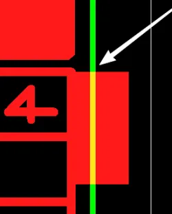
Figure 1: Copper extending beyond the defined board outline
We suggested adjusting the outline by routing 0.2mm on one side to prevent copper rolling and burr formation during depanelization. If ignored, exposed copper edges could result after mechanical routing or V-scoring, leading to potential short circuits during assembly or cosmetic defects that fail IPC-A-600 visual acceptance criteria. In severe cases, copper burrs may cause handling damage or reliability issues in edge-sensitive applications.
Our engineer recommended this modification because the current configuration risked copper rollover defects, especially with the customer's self-depanelization requirement. The adjustment ensures clean edges on the finished 5pcs shipment.
Panelization Strategy Confirmation
The original data showed 1×1 panelization, but based on previous orders for this customer, we proposed a 1×5 array with shipping dimensions of approximately 224 × 163.8mm. This change improves material utilization and process efficiency while maintaining the requested final board size.

Figure 2: 1×5 panelization
Confirming panelization early avoids downstream issues in routing and testing. Without alignment on this, mismatched array layout could lead to incorrect breakout tabs or increased scrap during customer depanelization.
Solder Mask & Silkscreen Issues
Top Layer Legend Size Too Small
The top-layer silkscreen features were designed too small for reliable printing with standard processes. Our team referenced previous successful runs and proposed enlargement to ensure legibility and adhesion after ENIG processing.

Figure 3: Too small top-layer silkscreen
If left unchanged, tiny legends risk incomplete ink transfer or smearing, resulting in unreadable markings that complicate assembly and quality inspection. We have seen cases where overly fine silkscreen leads to additional touch-up work or customer rejection.
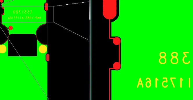
Figure 4: Updated marking
Bottom Layer Solder Mask Modification Request
The customer requested deletion of certain traces and characters from the bottom solder mask layer, along with addition of factory code and UL marking. Since our UL certification for this setup was inactive, we proposed adding only the factory code to maintain traceability without introducing compliance risks.
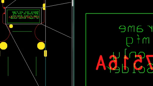
Figure 5: Suggested factory code and UL marking
Inconsistent fabrication notes between layers can cause confusion in production. Our CAM engineer confirmed the deletion while ensuring solder mask integrity around critical features to prevent solder bridging or exposed copper risks.
Stackup & Material Issues
Lamination Structure and Thickness Confirmation
After reviewing the stackup, we referenced previous production data and proposed a finished thickness of 1.55mm ±10% to better align with standard symmetric 4-layer builds using the provided core and prepreg materials. This helps control warpage and ensures compliance with overall thickness tolerances.
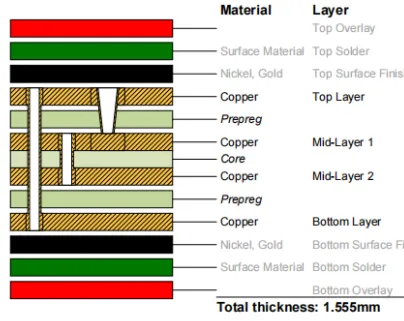
Figure 6: Stackup and finished thickness info
Without confirmation, deviation from expected thickness could affect impedance (if later required) or mechanical fit in enclosures. We always verify stackup early because asymmetric copper distribution or improper prepreg selection can lead to board warpage, especially in TG170 material under thermal stress during assembly.
Manufacturing Risks and DFM Insights
This case highlights several recurring DFM challenges. Copper features too close to or beyond the outline are common when designers use tight keep-out rules without considering routing tool compensation. Ignoring the 0.2mm adjustment could have resulted in exposed copper on edges after depanelization, increasing shorting risk during handling or conformal coating application.
Legend sizing issues often stem from CAD settings optimized for visual review rather than manufacturing capabilities. Small characters may pass DRC in design software but fail in actual screen printing, leading to yield loss or extra engineering time.
Panelization mismatches between orders cause unnecessary communication loops and potential data errors. In high-volume scenarios, this can delay production by days. The bottom layer modification request also underscores the importance of clear layer-specific instructions to avoid misinterpretation.
How the Engineering Team Resolved the Issues
Our team promptly raised targeted EQs with annotated screenshots for each issue. For the copper overhang, we provided a modified outline proposal and requested confirmation to avoid copper rollover. The customer quickly approved the 0.2mm adjustment.
Legend enlargement followed precedents from prior jobs, and panelization was standardized to 1×5 for consistency. Stackup and thickness were aligned with historical data, reducing risk of warpage. Factory code addition was implemented without UL marking to maintain compliance.
Throughout the process, we maintained clear communication, providing updated files where necessary. This collaborative approach minimized iterations and allowed the order to move forward within the 14-day window.
Final Manufacturing Outcome
All engineering questions were resolved with customer confirmation. Production data was updated accordingly: outline adjusted, panelization confirmed, legends enlarged, bottom layer cleaned per request, and stackup verified. The order was approved for production with 100% flying probe testing and standard process controls in place. CAM review was completed successfully, and boards were released for fabrication.
Key Takeaways for PCB Designers
- Always define board outlines with sufficient clearance (typically 0.2mm or more) from copper features to accommodate routing tolerances and prevent edge defects.
- Verify silkscreen minimum feature sizes against your fabricator's capabilities — 0.15–0.2mm line width is often safer for reliable printing.
- Maintain consistency in panelization across repeat orders and clearly document any customer-specific requirements.
- Provide layer-specific fabrication notes and avoid conflicting instructions between solder mask and copper layers.
- Reference previous job numbers or stackup history when placing repeat orders to speed up engineering validation.
- Include clear hole attributes and tolerance expectations in fabrication drawings to reduce ambiguity during CAM processing.
FAQ
Q1: Why is copper overhang beyond the board outline a problem?
A1: Copper extending past the outline can roll over or create burrs during routing or V-cutting. This leads to exposed copper on finished board edges, which may cause shorts, handling damage, or failure to meet IPC-A-600 cleanliness and edge quality standards.
Q2: How small can solder mask legends be reliably produced?
A2: Minimum reliable legend width depends on the process but is typically 0.15–0.25mm. Smaller features risk incomplete printing or poor adhesion, especially after surface finish. Fabricators often enlarge based on proven parameters to ensure readability.
Q3: Why confirm panelization even for small quantities?
A3: Proper panelization improves material utilization, routing efficiency, and testing consistency. Mismatches can cause incorrect board dimensions after depanelization or increased scrap risk.
Q4: What happens if stackup and thickness are not confirmed early?
A4: Unverified stackups may lead to warpage, thickness out of tolerance, or impedance deviations. Early confirmation with reference to previous runs helps align material selection and lamination parameters.
Q5: Why do CAM engineers sometimes remove or modify elements on specific layers?
A5: Modifications ensure manufacturability and compliance. For example, conflicting traces in solder mask or inactive markings (like expired UL) are adjusted to prevent defects or regulatory issues while preserving functionality.






