In PCB manufacturing, even straightforward-looking orders can hide significant manufacturability challenges. This case involves a 4-layer FR-4 Motor Stator board with heavy 6oz copper, 2.5mm thickness, and tight mechanical features. During our standard CAM engineering review, several critical issues emerged that required customer clarification to prevent production defects.
Heavy copper designs for motor applications bring unique demands on etching, plating, and mechanical processing. Our CAM team routinely identifies gaps between design intent and factory capabilities. In this project, we raised multiple EQs focused on edge pad proximity, tooling hole requirements for small vias/holes, solder mask inconsistencies, and fabrication data mismatches. These clarifications helped avoid potential yield loss and assembly problems downstream.
Order Overview
This was a single-piece 115mm x 115mm 4-layer PCB fabricated on FR-4 (KB-6165F equivalent, TG150) with 2.5mm finished board thickness(#FR4-20260113-014). Outer and inner copper weights were specified at 6oz, presenting notable etching and registration challenges. The design included a minimum hole size of 0.3mm and required 100% flying probe testing. Surface finish was lead-free HASL, with green solder mask and white silkscreen. Panelization was 1x1 with mechanical routing, no V-CUT initially noted. Delivery target was 18 days for 100 pieces.
The board was intended for a Motor Stator application, where high current carrying capacity from the heavy copper and mechanical stability are critical. No impedance control was specified, but the thick board and heavy copper demanded careful stackup verification and process control to manage warpage and copper distribution uniformity.
Main Engineering Questions Found During CAM Review
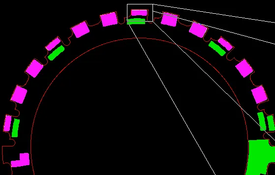
1. Pads Too Close to Board Edge – Risk of Copper Exposure After Routing
We noticed several highlighted pads positioned very close to the board outline in the Gerber data. Our engineer flagged this because the standard routing process, including milling tolerances and potential panel breakout, could result in exposed copper at the edges.
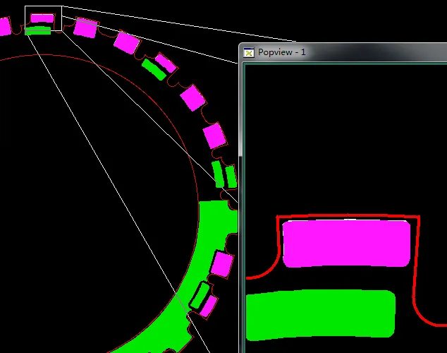
Figure 1: Highlighted pads are very close to the board outline in the Gerber data
According to typical IPC-A-600 acceptability criteria, exposed copper near the board edge increases the risk of edge shorting during assembly or in the field, especially in motor stator environments with vibration and potential contamination. If ignored, this could lead to copper peeling, short circuits between layers or to chassis, or cosmetic defects that fail final inspection. In worst cases, it results in scrap boards or field failures after assembly.
We asked the customer to confirm the clearance intent and suggested minor adjustment to the copper keep-out or board outline if feasible. This is a common DFM issue in compact motor control boards where designers maximize component area without accounting for mechanical processing tolerances.
2. Small Hole Size (0.35mm) and Lack of Production Tooling Holes
The board featured primarily 0.35mm holes, which are too small to serve reliably as production fiducials or positioning holes. Our CAM engineer identified that without dedicated tooling holes, panel alignment during drilling, routing, and testing could be compromised, leading to registration errors and drill breakout.
We recommended adding three 2.0mm non-plated holes inside the board area for production positioning. If this was not addressed, misalignment during multi-step processing could cause via cracking, open circuits, or inconsistent hole wall quality – particularly risky with 6oz copper where plating aspect ratios are already challenging. Yield loss in heavy copper boards from such issues can exceed 20-30% in extreme cases.
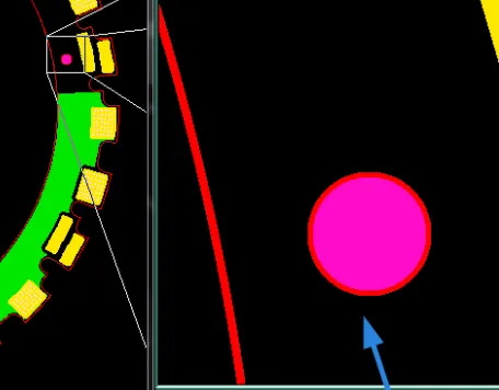
Figure 2: Recommended 2.0mm non-plated hole inside the board area
The customer confirmed the addition, and our team incorporated these non-functional holes into the manufacturing data. This adjustment aligns with standard factory practices for boards lacking sufficient large features for reliable fixturing.
3. Solder Mask and Silkscreen Data Inconsistencies
In the provided Gerber files, 0.35mm holes showed solder mask openings on both top and bottom layers, while the fabrication notes specified bottom layer cover (tented vias or mask-defined). Additionally, top layer silkscreen included both negative and positive elements, while bottom was negative only. Surface finish notes also showed minor conflicts.
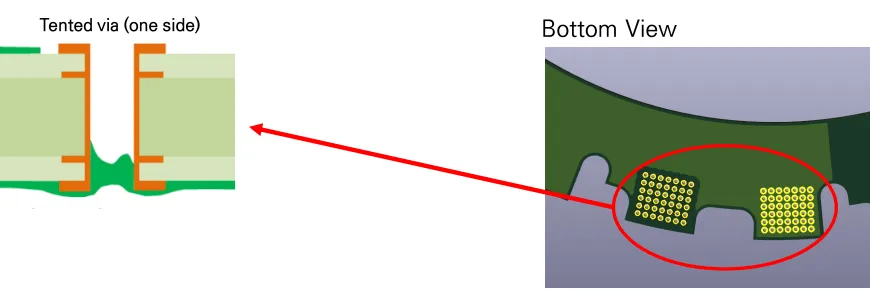
Figure 3: Tented vias from the bottom view

Figure 4: Surface finish note
We confirmed these points with the customer because mismatched data can lead to incorrect solder mask application, resulting in poor solderability, bridged pads, or exposed traces where protection was intended. For a Motor Stator board, inconsistent mask could cause solder wicking issues or contamination paths.
Our engineer suggested aligning the Gerber to the dominant fabrication note (bottom covered) and clarifying silkscreen intent. Ignoring this would likely produce boards with functional or cosmetic defects, requiring rework or rejection.
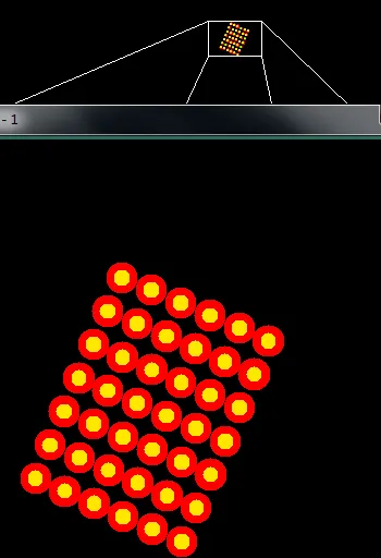
Figure 5: Solder mask openings on double sides
4. Stackup and Dimension Confirmation
We provided our recommended stackup based on the 2.5mm thickness and 6oz copper requirements and asked for confirmation. Dimensions in the notes also needed cross-check against Gerber. These steps are standard to ensure registration and copper balance for thick, heavy copper boards prone to warpage.
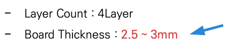
Figure 6: Layer and board thickness info

Figure 7: 6oz copper requirement
Heavy copper stackups can suffer delamination or excessive bow/twist if copper distribution is unbalanced. We adjusted prepreg and core selections accordingly after confirmation.
Suggested EQ Categories
File & Manufacturing Data Issues
- Gerber vs. fabrication note inconsistencies (holes, surface finish, dimensions)
- Silkscreen layer polarity differences between top and bottom
Hole & Tolerance Issues
- Insufficient production positioning holes for 0.35mm minimum holes
- Drill size and plating considerations for small features
Panelization & Process Optimization
- Pad-to-edge clearance for routing safety
- Factory code placement on top layer silkscreen
Stackup & Material Issues
- Heavy copper 6oz stackup verification for 2.5mm thickness
Manufacturing Risks and DFM Insights
This case highlights several recurring DFM pitfalls in motor-related PCBs. Designers often underestimate routing and milling tolerances when placing pads near board edges. In heavy copper boards, this is amplified because thicker copper requires more aggressive etching, widening the effective clearance needed.
Small hole sizes without auxiliary tooling holes frequently trigger EQs because flying probe and CNC routing rely on accurate fixturing. Without them, cumulative registration errors can cause via-to-pad misalignment, leading to open circuits or unreliable plating – failures that only appear during electrical testing or assembly.
Data inconsistencies between Gerber and notes are common but dangerous. They force CAM engineers to pause production and seek clarification, extending lead times. In this order, multiple such issues risked producing non-functional boards with incorrect solder mask or silkscreen, directly impacting solderability in the stator assembly process.
How the Engineering Team Resolved the Issues
Our team worked closely with the customer through annotated screenshots. For the edge pads, we proposed and received approval to adjust clearance where possible while maintaining design functionality. We added the three 2.0mm tooling holes in non-critical areas after confirmation.
Stackup was finalized based on our recommended build-up to balance copper and control thickness. Solder mask and silkscreen files were synchronized to match the primary fabrication notes. All changes were documented in the engineering file for traceability.
We also added the factory code in the specified top layer position. These optimizations reduced mechanical and plating risks while keeping the board within standard FR-4 processing windows.
Final Manufacturing Outcome
After receiving customer approvals on all EQ points, the manufacturing data was updated, and the job was released for production. The panelization, drill programs, and imaging files were finalized with the confirmed tooling holes and clearances. The order proceeded through lamination, drilling, plating, and testing without further issues, meeting the 18-day delivery window.
Key Takeaways for PCB Designers
- Always include at least 2-3 large non-plated tooling holes (1.5-2.5mm) when minimum hole size is below 0.4mm to ensure reliable production fixturing.
- Maintain adequate copper-to-edge clearance (typically 0.5mm or more depending on routing method) to prevent exposed copper after depanelization.
- Ensure Gerber files fully match fabrication notes, especially for solder mask openings, silkscreen polarity, and surface finish requirements.
- For heavy copper designs (>3oz), provide clear stackup drawings early and expect potential adjustments for copper balance and warpage control.
- Define layer stackup and drill attributes clearly in both Gerber/ODB++ and accompanying documentation to minimize interpretation errors.
- Review board outline and mechanical features against copper pour patterns during layout to catch edge proximity issues early.
- Use consistent naming and polarity across all layers to avoid silkscreen or mask mismatches.
FAQ
Q1: Why do PCB factories require additional tooling holes when holes are small (0.35mm)?
A1: Small holes lack sufficient mechanical strength and accuracy for panel positioning during drilling, routing, and testing. Dedicated larger non-plated holes provide reliable fiducials, preventing misalignment that can cause drill breakout or registration failures.
Q2: What risks arise from pads placed too close to the board edge?
A2: Routing or milling tolerances can expose copper, leading to shorts, corrosion, or assembly problems. In vibration-heavy applications like motor stators, this significantly raises field failure risk.
Q3: Why must solder mask data match fabrication notes exactly?
A3: Mismatches result in unintended openings or coverage, causing solder bridging, poor wetting, or exposed traces. CAM engineers must resolve these to produce boards that meet both electrical and mechanical requirements.
Q4: How does heavy copper (6oz) affect DFM decisions?
A4: It increases etching undercut, registration difficulty, and warpage potential. Stackup balancing and clearance rules become stricter to maintain yield and dimensional stability.
Q5: What is the purpose of adding factory codes on silkscreen?
A5: It aids internal traceability during production, quality control, and after-sales support without interfering with customer assembly.
Q6: Can these issues be avoided in the design phase?
A6: Yes, by following DFM guidelines for edge clearance, including tooling holes, and performing a thorough design rule check against the target manufacturer's capabilities before releasing Gerbers.