


Engineering Cases
Engineering Cases focuses on real PCB engineering reviews, manufacturing challenges, and production optimization processes from actual fabrication projects. This category highlights how different PCB designs are evaluated and adjusted during engineering review, covering topics such as stack-up analysis, impedance control, drill optimization, copper balancing, solder mask alignment, DFM review, and production risk assessment across various PCB applications. The content in this section is based on practical manufacturing scenarios rather than theoretical introductions. Each engineering case demonstrates how specific PCB issues are identified, analyzed, and resolved during production preparation and fabrication. These records help engineers, purchasers, and hardware teams better understand the relationship between PCB design decisions and manufacturing stability, yield control, and process reliability. Topics may include multilayer PCB engineering review, HDI process optimization, flexible PCB manufacturing considerations, heavy copper processing adjustments, surface finish selection, Gerber data verification, and other real-world PCB production experiences. By organizing engineering challenges and process solutions into structured case content, this category provides valuable insight into practical PCB manufacturing and engineering workflow management.
Featured Blog
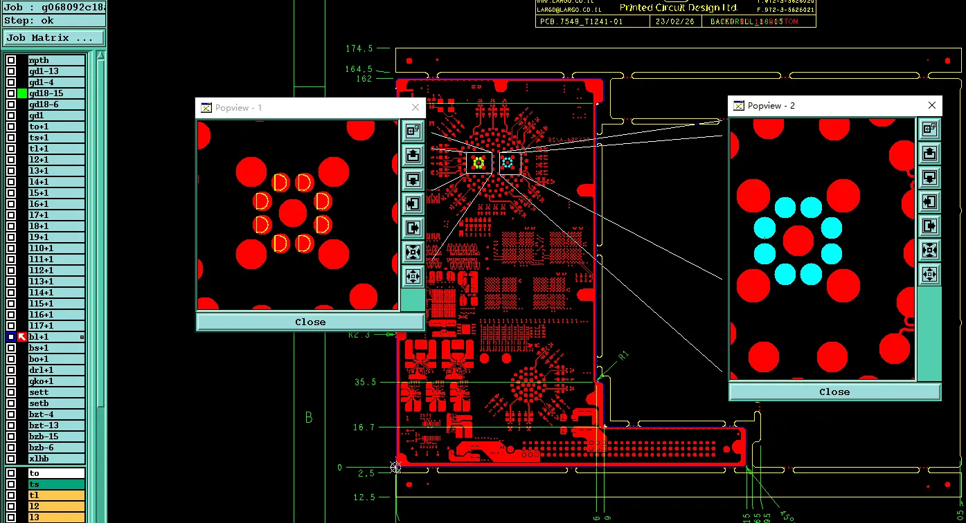
PCB Hole Attributes and Special Drilling: Common CAM Review Conflicts
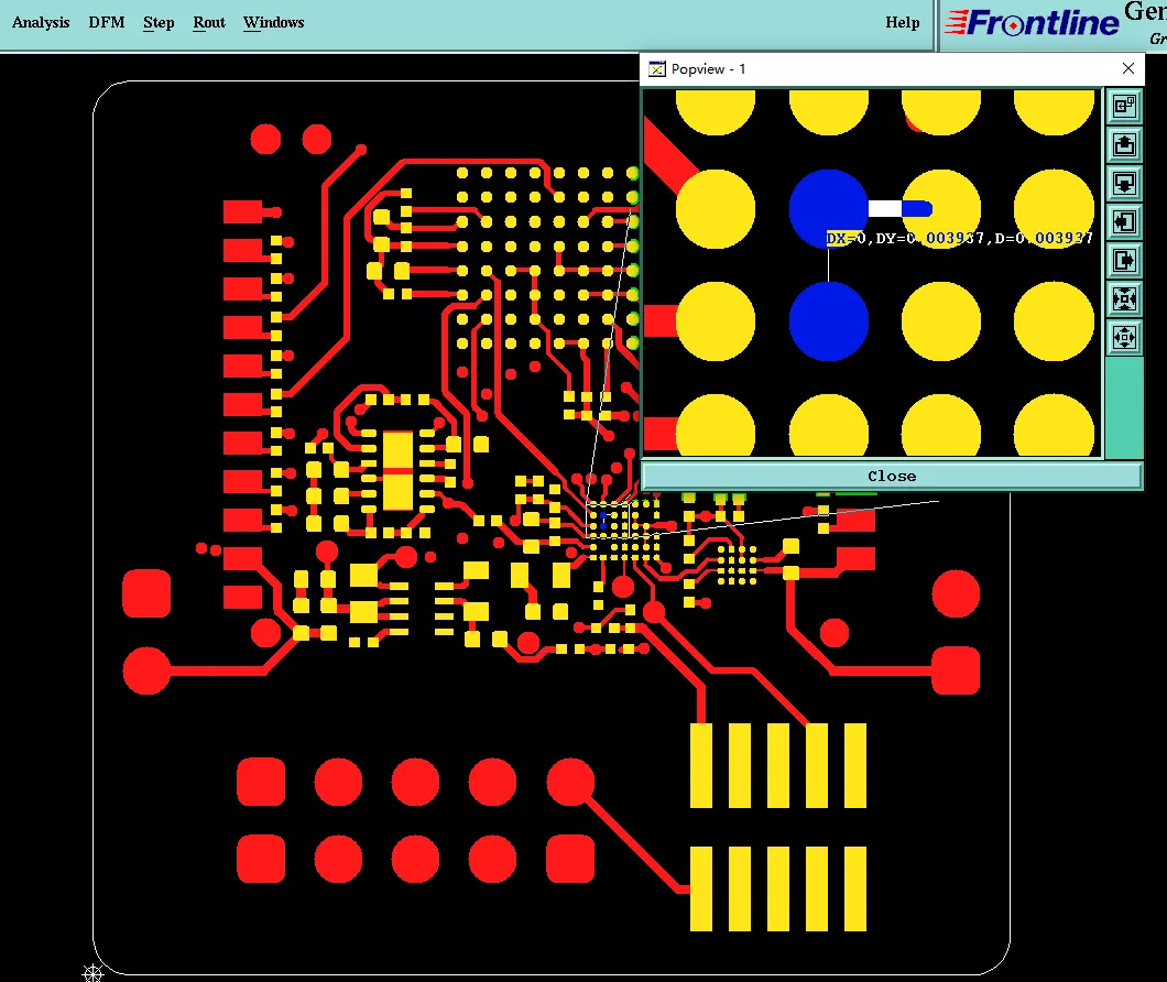
See how CAM reads PCB hole attributes and special drilling—PTH vs NPTH, back drill, press-fit holes, countersink, and laser vias—and why incomplete data delays fabrication.
Latest Blogs
PCB Press-Fit Hole Design Rules for Heavy Copper Boards
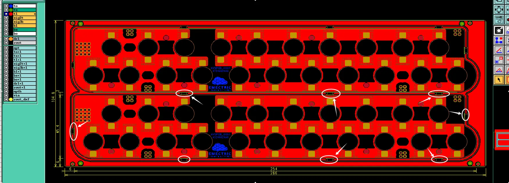
Learn why a 4-layer 3 oz copper PCB with unspecified press-fit hole finished size and large 12.5 mm NPTH openings required process capability evaluation before production release.
How We Resolved Missing Stamp Holes in 2-Layer Panel
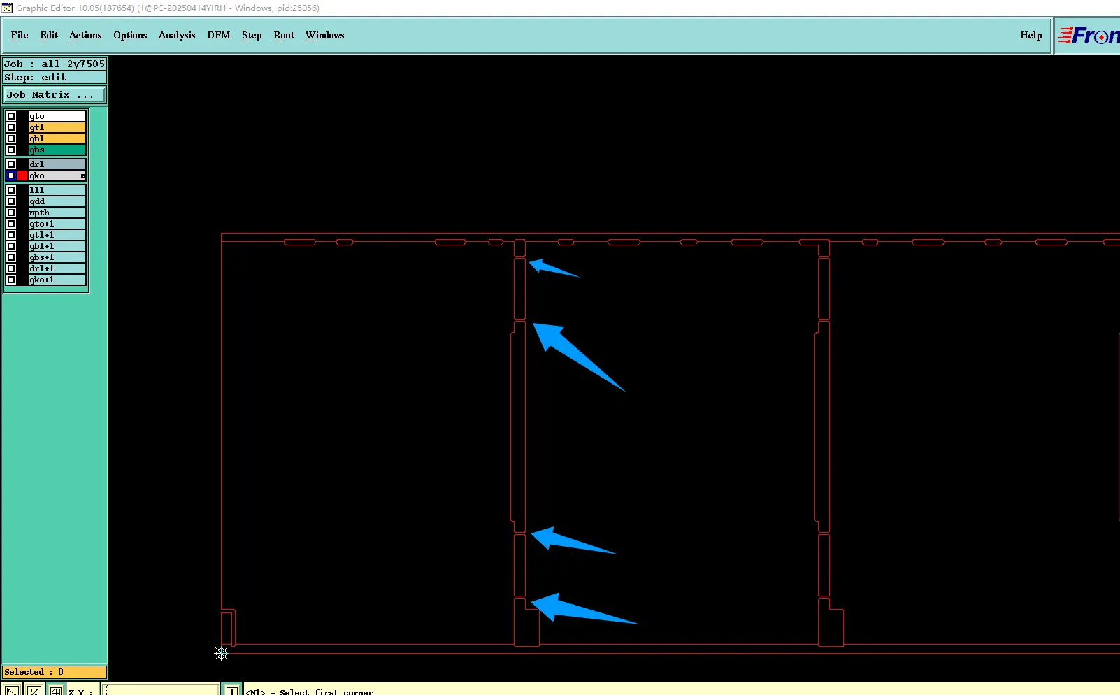
CAM review of a large 2-layer FR-4 V-cut panel with zero process edge found solid connection tabs missing stamp holes. Adding standard stamp-hole rows prevented in-process breakage and ensured clean depanelization before production release.
FPC Stiffener Design Rules: Avoiding Insertion Finger Failure
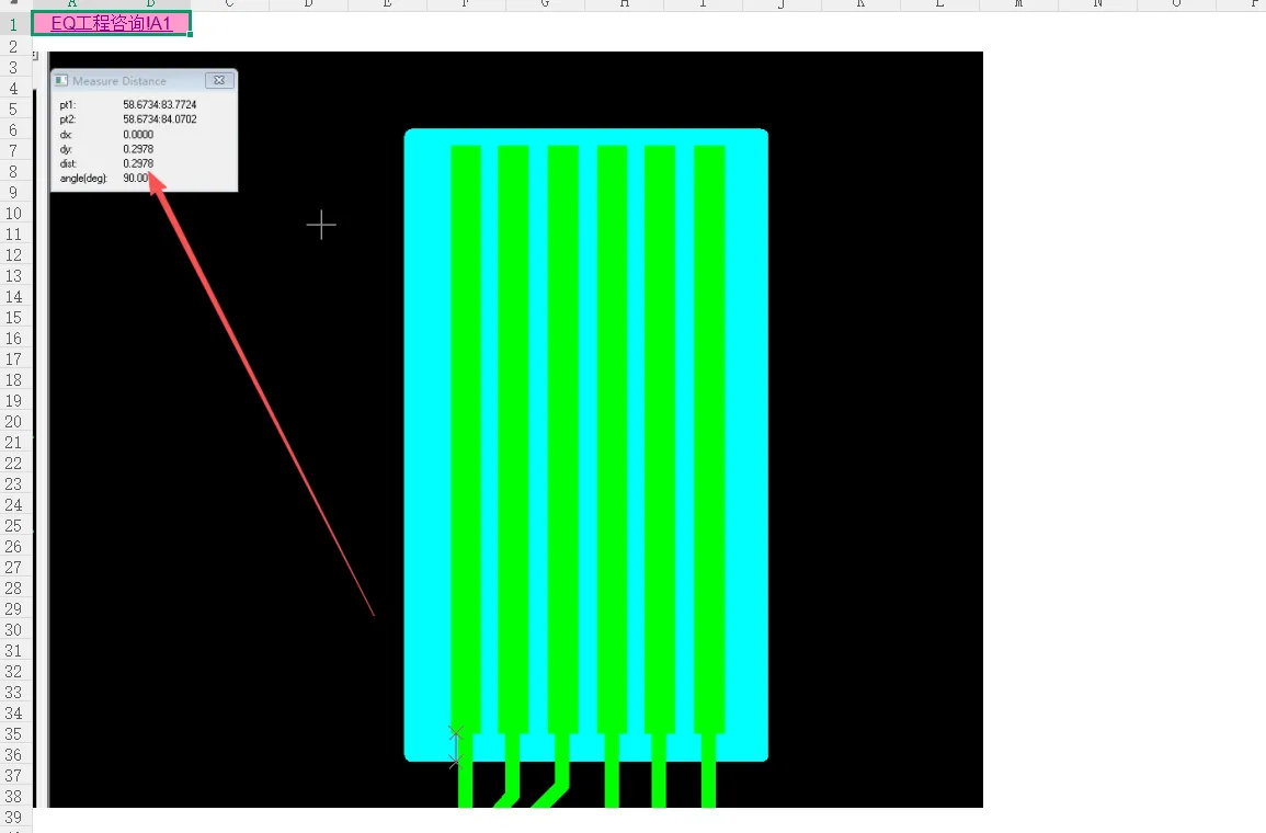
Discover why FPC stiffener design rules for PI stiffener-to-finger clearance, 0.15mm copper pullback, and GM/GM1 outline consistency required process capability evaluation to prevent finger breakage and gold exposure on 0.2mm laser-cut flex PCBs.
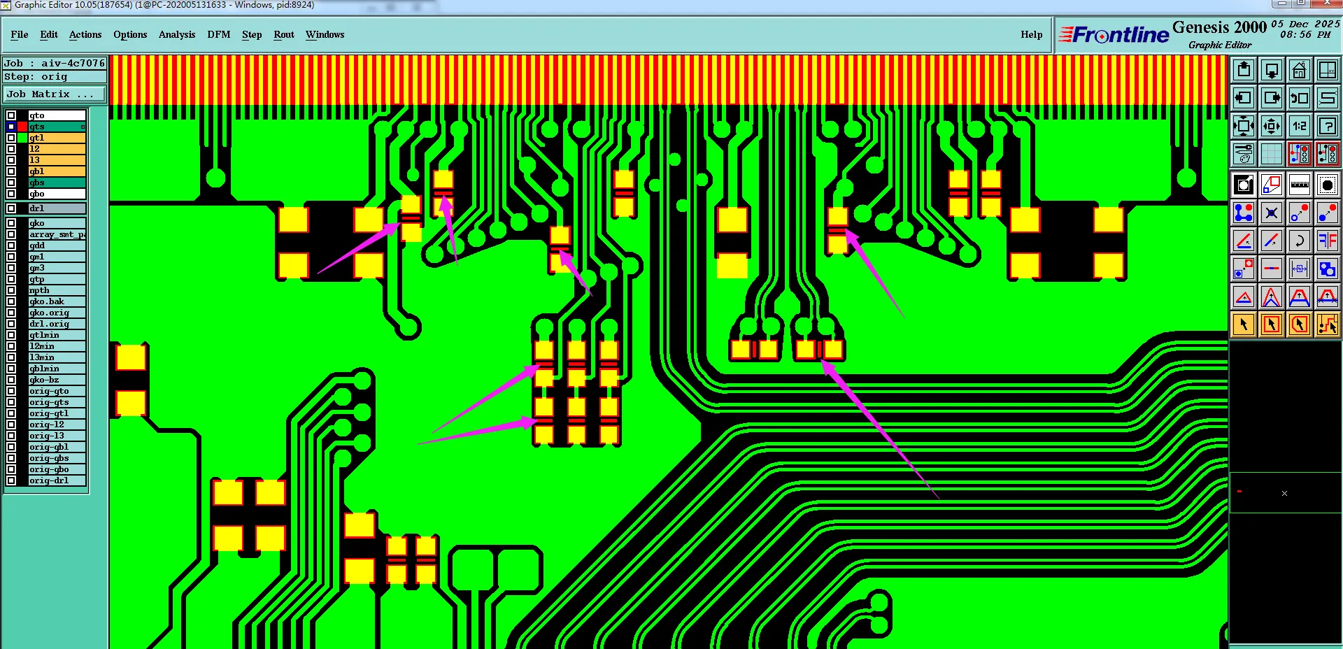
How DFM Prevented SMT Shorts from Narrow Mask Bridges
This case shows how DFM review used PCB Solder Mask Bridge Minimum Width rules on a thin 4-layer FR-4 board to convert fine-pitch gaps below 0.18 mm into full openings, stopping solder bridges and protecting SMT yield.
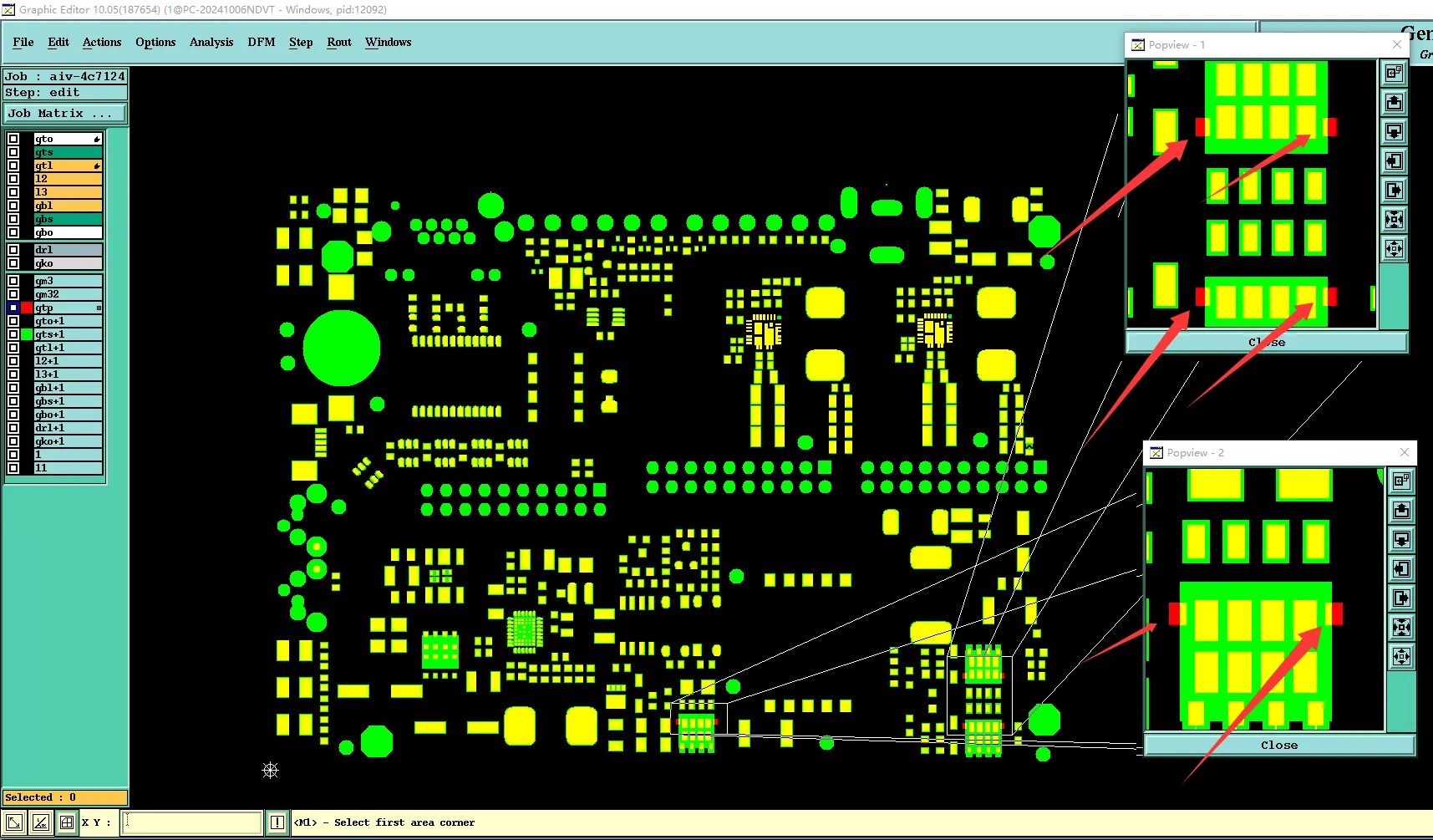
Solder Mask vs. Paste Mask: Perfecting Your Opening Design
CAM review of a 4-layer FR-4 panel found solder mask openings larger than paste apertures exposing traces. Corrections copied paste geometry and covered traces to prevent solder wicking before immersion gold and assembly.
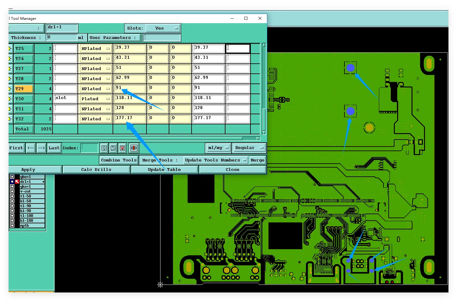
PCB Via-in-Pad Design Rules: Avoiding SMT Assembly Voids
This PCB Via-in-Pad Design Rules case shows how DFM review stopped open vias inside SMT pads on a 4-layer FR-4 board from causing solder wicking and cold joints, while fixing edge clearance and mask bridge risks for reliable assembly.
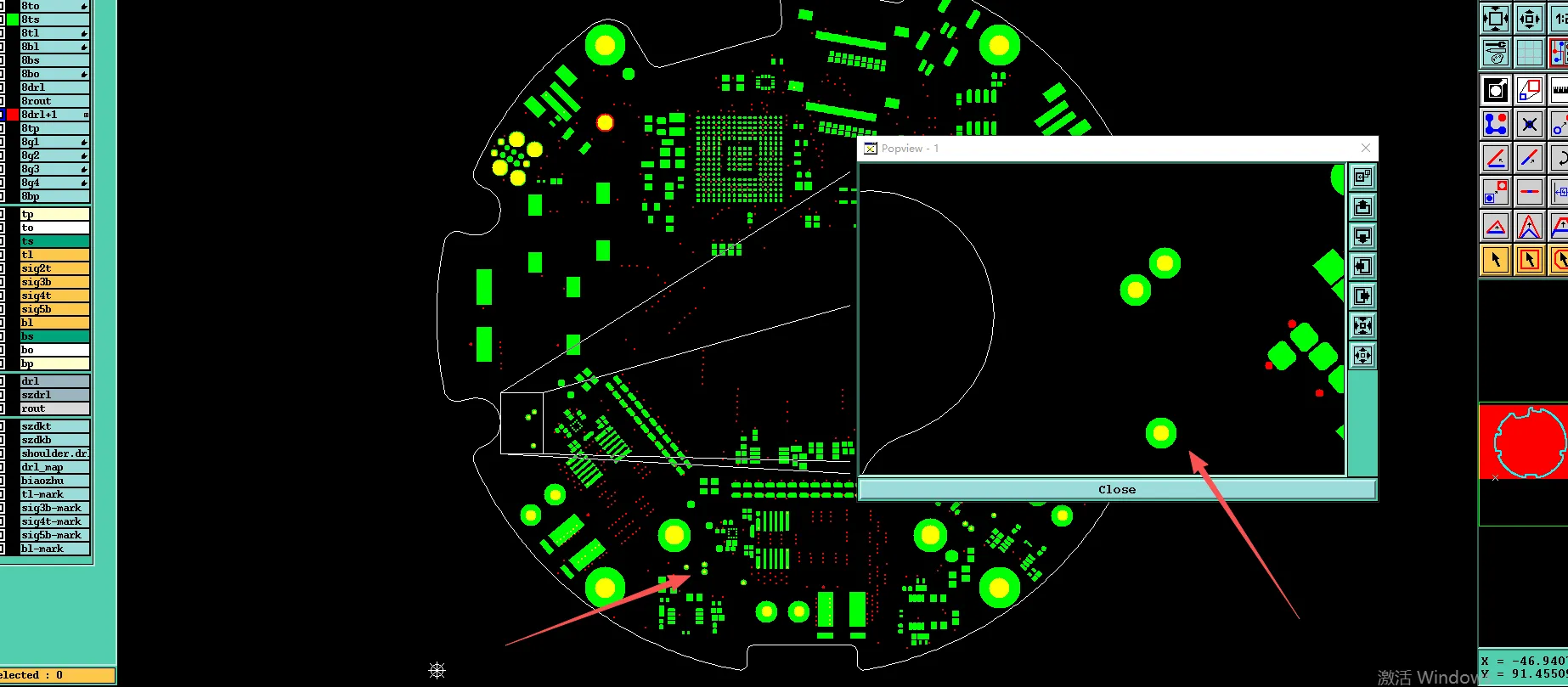
Avoiding DFM Delays: A Guide to PCB Resin Filled Via Design
CAM review of a 6-layer FR-4 ENIG panel found selective 0.25 mm resin plug notes conflicting with full via population needs. Clarification extended non-conductive resin filling to all vias for surface planarity and process consistency before production.
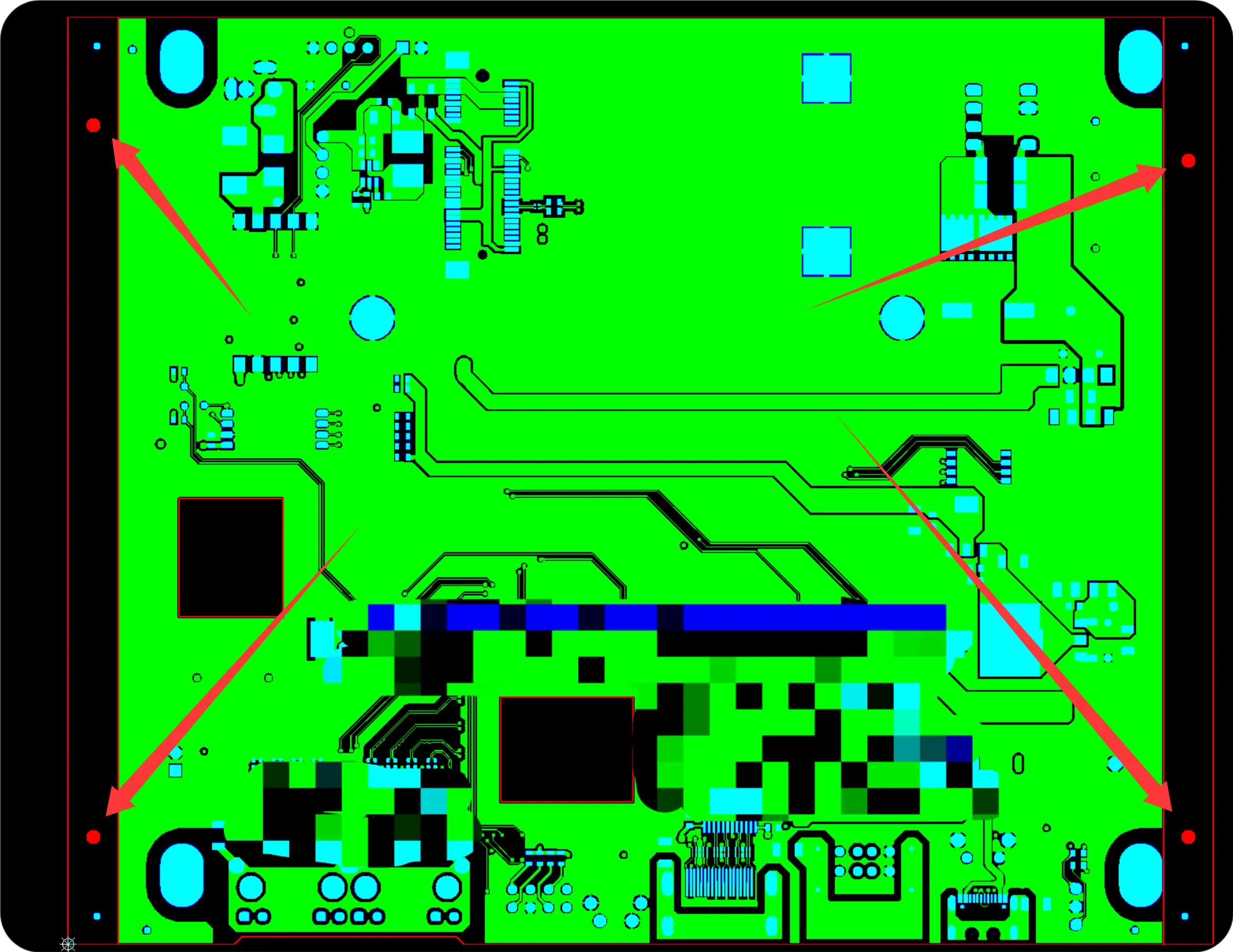
Handling PCB Impedance Trace Width Adjustment in DFM Review
Discover why PCB impedance trace width adjustment from 5 mil to 7 mil was essential for single-ended impedance control on a 4-layer 1 oz FR4 board, plus black solder mask bridge limits, tooling holes and edge-pad clearance for reliable process capability.
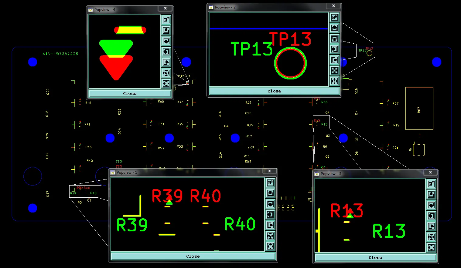
Aluminum PCB Design Guidelines: Essential DFM Rules for LEDs
This Aluminum PCB Design Guidelines case shows how DFM review fixed tight trace clearances on a single-sided MCPCB, preventing shorts, converting an oversized hole to routing, and protecting high-voltage yield and reliability.
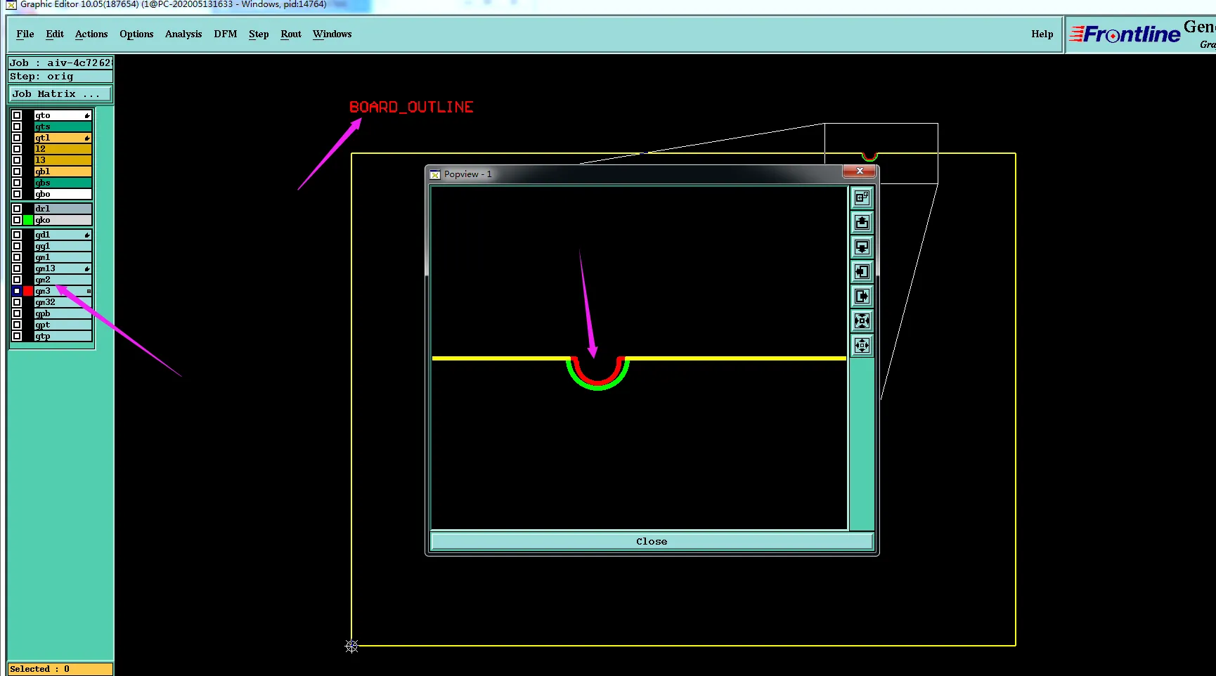
PCB Outline Layer Definition: Avoiding Gerber File Ambiguity
CAM review of multi-file Gerber data revealed competing GM1 and GM3 outline layers plus slot mismatches with the drill file. Clarification locked one production file and GM3 as the authoritative contour to prevent incorrect board outlines and cut-outs.
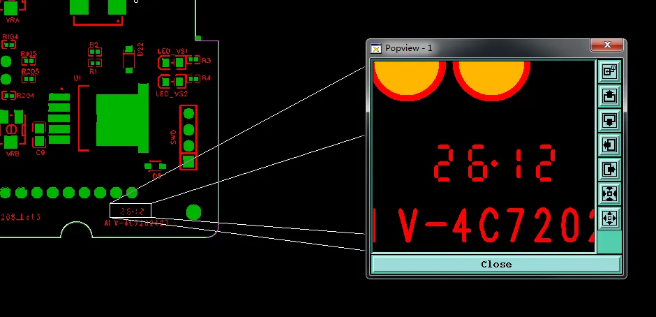
Optimizing PCB Production Markings for Traceability
Learn how CAM engineers optimized PCB production markings by placing year-week date codes and serial numbers on process rails. This ensures lot traceability, meets IPC Class 3 needs, and enables seamless sample-to-mass production transition.
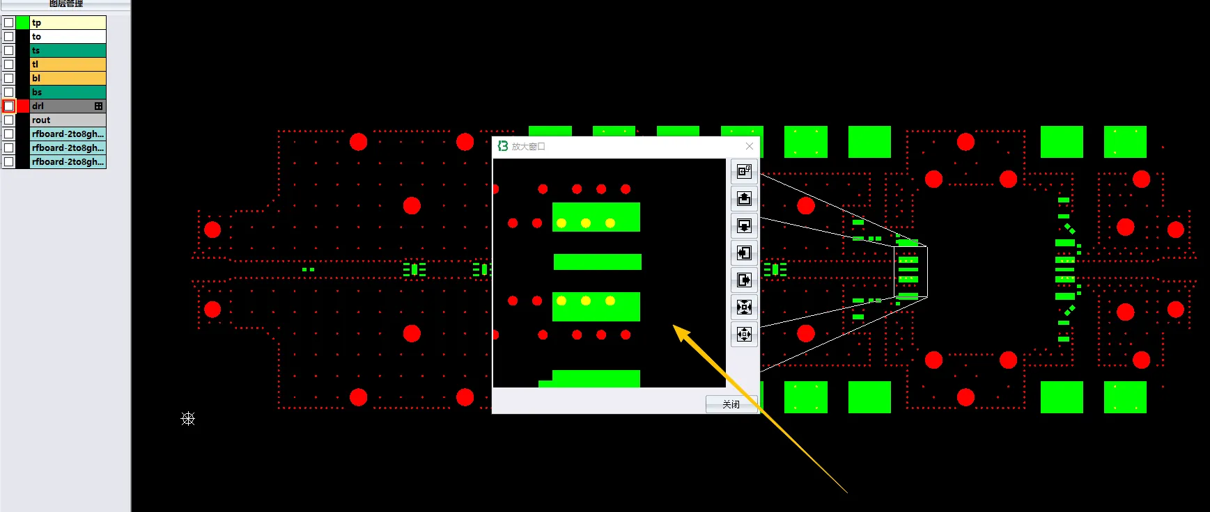
Rogers 4350B PCB Design Guide: Avoiding Via-in-Pad SMT Failures
This Rogers 4350B PCB Design Guide explains how DFM review stopped Via-in-Pad voids, substrate yellowing, and edge copper exposure on a thin high-frequency board, protecting solder joints and assembly yield.


