In this real-world CAM engineering case, we processed a 4-layer 1.6mm FR-4 TG170 board with 2oz copper on both inner and outer layers. The order involved 2040 pieces (340 sets) using a 3x2 panelization with V-CUT depanelization. During the standard DFM review, several critical manufacturing clarification points emerged that required direct customer confirmation before releasing the job to production.
This case highlights the typical gaps between customer design files and actual fabrication requirements, especially for medium-volume runs where both quality and delivery speed matter. Our CAM team identified issues related to stackup definition, process edge reinforcement, production traceability, and data consistency with previous versions.
4-Layer 2oz FR-4 TG170 PCB Order Specifications and Panelization
The PCB (#FR4-20260317-052) measured 55 × 70 mm per single piece, built on 4 layers using FR-4 material (KB-6167F equivalent) with a glass transition temperature of TG170. Finished board thickness was specified at 1.6mm, with 2oz copper weight on both inner and outer layers. Surface finish was immersion gold (ENIG) with 1.0μm minimum thickness. Solder mask was green on both sides, and silkscreen was white.
Minimum hole size was 0.8mm. The panelization used a 3x2 array with V-CUT + routing combination for depanelization. Total panel count was 340 sets. No impedance control was required, and there were no BGAs. Electrical testing was to be performed using an engineering test fixture. The job was marked for production confirmation, supplied through Aivon with factory reference AIV-4C7202389.
This configuration is common for industrial control or power supply applications, but the combination of 2oz copper, V-CUT panelization, and unspecified stackup details triggered multiple engineering questions during CAM review.
Critical DFM Issues Identified in 4-Layer FR-4 TG170 PCB CAM Review
1. Missing Stackup Definition and Factory Standard TG170 Material Proposal
The most significant issue we encountered was the complete absence of a detailed layer stackup in the customer's fabrication data. For a 4-layer board with 1.6mm finished thickness and 2oz copper, this is critical because dielectric thicknesses directly affect impedance (even if not controlled), registration, and warpage behavior.
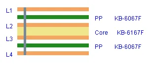
Figure 1: 4-layer board stackup information
Our engineer noted: "We noticed no stackup was provided. In order to meet the 1.6mm board thickness requirement while using readily available high-TG material, we will apply our standard factory stackup unless otherwise specified." We proposed using our common TG170 FR-4 materials with symmetric construction to minimize warpage risk.
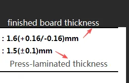
Figure 2: The finished board thickness (1.6mm) vs laminated thickness
If this had been ignored and production continued with mismatched dielectrics, the board could have suffered from excessive bow and twist, leading to assembly issues or even delamination under thermal stress during reflow. According to typical IPC-2221 guidelines for multilayer construction, unbalanced stackups with thick copper layers increase warpage probability significantly.
| Layer | Copper Weight | Key Consideration |
|---|---|---|
| Outer Layers | 2oz | Symmetry for warpage control |
| Inner Layers | 2oz | Dielectric matching to 1.6mm total |
Table 1: 4-Layer 1.6mm FR-4 TG170 Stackup Recommendation
2. V-CUT Panelization and Process Edge Reinforcement for Panel Stability
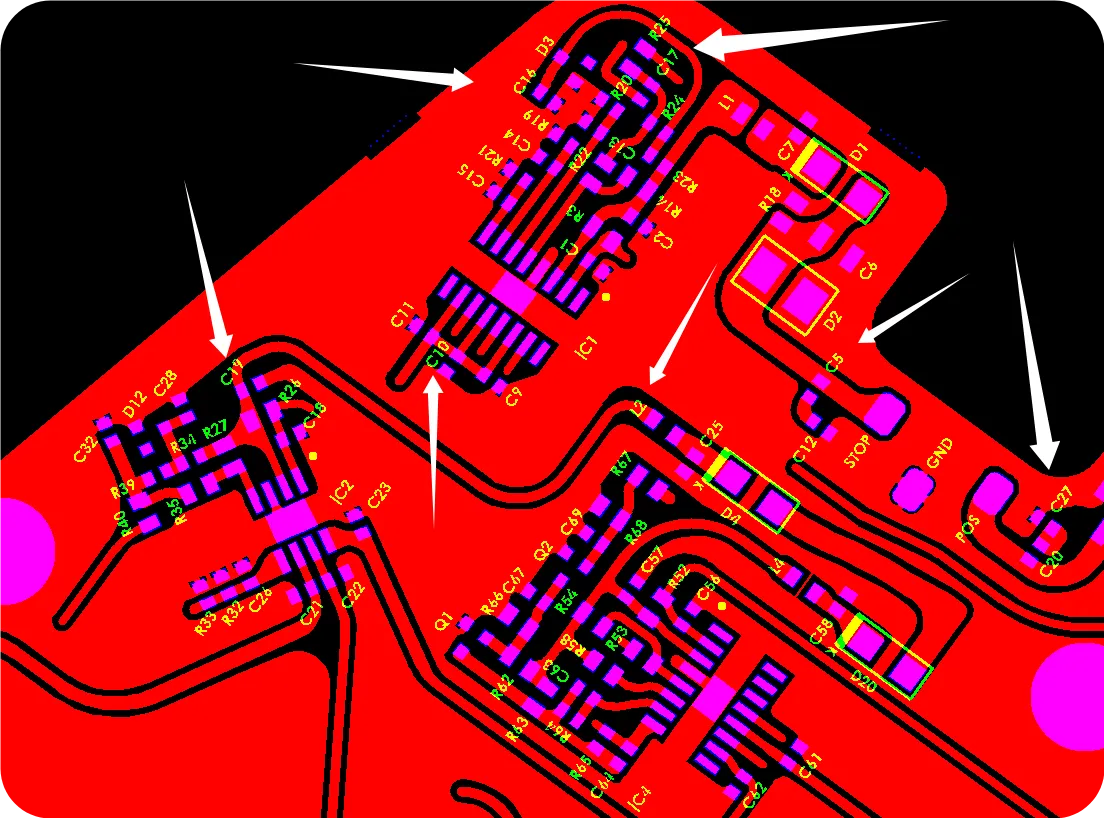
The panelization was specified as 3x2 with V-CUT. Our CAM team identified that the customer's process edge design lacked sufficient inner layer copper reinforcement. We suggested adding diamond-pattern copper pour on inner layers and a protective copper ring on outer layers along the process edges.
Figure 3: 3x2 panelization with V-CUT
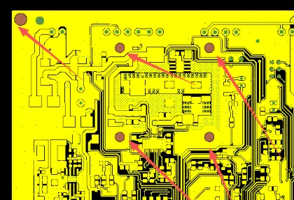
Figure 4: Diamond-pattern copper pour on inner layers
Our engineer suggested adjusting the copper clearance because we noticed the V-CUT area was too close to exposed copper features in some areas. This reinforcement improves panel rigidity during lamination and handling, especially important for 2oz copper boards which are heavier and more prone to flexing.
Figure 5: Copper clearance between V-CUT area and inner layers
Had this not been addressed, there was a high risk of panel deformation during press lamination, resulting in layer-to-layer misalignment or even resin voids near the edges. Post-depanelization, exposed copper near V-CUT lines could lead to shorting or cosmetic defects during assembly.
| Feature | Recommendation | Benefit |
|---|---|---|
| Inner Layer | Diamond-pattern copper pour | Improved rigidity during lamination |
| Outer Layer | Protective copper ring | Reduced deformation risk |
Table 2: V-CUT Process Edge Reinforcement Guidelines
3. Production Traceability Marking and Date Code Requirements
The customer had not specified any production numbering or date code requirements. Following our standard practice for traceability, we proposed adding a standard year-week code in a blank area of the silkscreen layer.
Figure 6: Standard year-week code in a blank area of the silkscreen layer
We also confirmed consistency with the previous version regarding additional numbering. The customer eventually confirmed no additional serial numbers were needed for this batch, which helped avoid unnecessary silkscreen clutter.
Figure 7: Required additional serial numbers
Without proper traceability marking, it becomes extremely difficult to track manufacturing lots if field issues arise months later. This is particularly important for TG170 boards used in reliability-sensitive applications.
4. Production Files vs Stencil Data Clarification
We provided the customer with our CAM-generated production files and PDF for confirmation, explicitly noting that these files were for engineering review only and not to be used for stencil creation. This is a standard precaution to prevent stencil misalignment caused by manufacturing compensations (such as solder mask expansion or trace adjustments).
Summary of DFM Engineering Questions by Category
File & Manufacturing Data Issues
- Missing detailed stackup definition
- Confirmation of production files vs. stencil files
- Consistency with previous revision data
Panelization & Process Optimization
- V-CUT + routing depanelization parameters
- Process edge copper reinforcement (diamond pour and guard ring)
- Panel utilization and handling strength
Traceability & Documentation
- Date code placement and format
- Production batch numbering policy
Key Manufacturing Risks for 2oz Copper 4-Layer TG170 PCBs
This case perfectly illustrates several common DFM pitfalls. The most frequent issue we see is incomplete stackup information. Without it, we must default to factory standards, which may not perfectly match the designer's intent. For 2oz copper 4-layer boards, improper dielectric selection can cause warpage exceeding IPC-A-600 limits, leading to assembly placement problems or solder joint stress.
V-CUT panelization on thicker copper boards requires careful process edge design. Without reinforcement, the panel can flex during lamination, causing registration errors that manifest as misaligned holes or breakout. If ignored, this often results in yield loss of 15-30% in extreme cases and potential scrap of entire panels.
Another insight is the importance of clear communication regarding traceability. Many customers assume default markings but later request changes, causing additional engineering cycles and potential delays.
EQ Resolution and Production File Optimization for TG170 Board
Our team promptly sent a detailed EQ package with marked-up drawings and proposed solutions. For the stackup, we provided our standard symmetric 4-layer construction using TG170 materials that would reliably meet the 1.6mm ±10% thickness requirement.
After customer confirmation on the process edge copper treatment, we implemented the diamond copper pour on inner layers and guard rings on outer layers. This significantly improved panel stability without affecting the functional circuitry.
Date code placement was agreed upon in a non-critical silkscreen area. All production files were re-verified after adjustments, and the job was released for tooling once final confirmation was received.
We also confirmed that this sample data would serve as the baseline for any future mass production runs of the same part number.
Successful Production Release After DFM Alignment
All engineering questions were resolved within the standard review window. The stackup was finalized using factory standard materials, process edges were reinforced, and traceability markings were applied per agreement. The job successfully passed final CAM verification and was released for production with optimized parameters for yield and reliability.
DFM Best Practices for 4-Layer 2oz FR-4 TG170 PCB Design
- Always provide a complete layer stackup drawing, especially for boards thicker than 1.0mm or with copper weights above 1oz.
- Include clear V-CUT and process edge requirements early in the design phase. Consider adding inner layer copper pour near panel edges for mechanical stability.
- Specify traceability requirements (date code, serial number, etc.) in fabrication notes to avoid last-minute changes.
- Clearly separate fabrication data from stencil data. Never use CAM production files directly for stencil creation.
- Reference previous revision numbers and highlight any intentional changes to reduce review time.
- For ENIG surface finish, pay special attention to isolated copper features and minimum feature sizes to avoid etching or plating issues.
- Verify minimum hole size (0.8mm in this case) against copper weight and aspect ratio early.
FAQ
Q1: Why is providing a detailed stackup so important for 4-layer boards?
A1: Without it, the factory must use standard materials which may not match your intended dielectric thicknesses. This can affect warpage, impedance (if relevant in future), and overall reliability. Clear stackup data allows precise DFM adjustments before production begins.
Q2: What risks occur if V-CUT process edges lack copper reinforcement?
A2: The panel may flex or deform during lamination and handling, leading to registration errors, layer misalignment, and potential delamination. After depanelization, exposed copper near cut lines can cause short circuits during assembly.
Q3: Why do CAM engineers recommend date codes even if not specified?
A3: Date codes provide essential traceability for quality control, failure analysis, and inventory management. Without them, identifying manufacturing lots in case of field issues becomes nearly impossible.
Q4: Can production files be used directly for stencil creation?
A4: No. Production files include manufacturing compensations (solder mask expansion, trace adjustments, etc.). Using them for stencils can cause misalignment and poor solder paste deposition. Always request dedicated stencil files from the manufacturer.
Q5: What is the typical tolerance for board thickness when not specified?
A5: Most factories apply ±10% tolerance per IPC standards for standard builds. For 1.6mm boards, this means 1.44mm to 1.76mm. Tighter tolerances require explicit specification and may affect material selection and cost.
Q6: How does 2oz copper affect DFM decisions compared to 1oz?
A6: 2oz copper increases etching difficulty, aspect ratio challenges for holes, and panel weight. It requires more careful design of minimum features, clearances, and process edge support to maintain high yield.