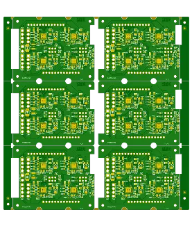
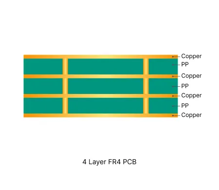
4 Layer FR4 PCB Production Record #FR4-20260317-052
| Parameter | Value | Parameter | Value |
|---|---|---|---|
| PCB Type | FR4 PCB | Quantity | 2040 pcs |
| Layers | 4 Layers | Board Type | Panel PCB |
| Dimensions | 55 x 70 mm | Copper Weight | 2oz |
| Thickness | 1.6 mm | Min Track / Spacing | 10/10mil |
| Surface Finish | ENIG (Immersion Gold) | Min Hole Size | 0.8mm↑ |
| Solder Mask | Green | Silkscreen | White |
| Stack-up | Custom | Impedance Control | No |
This 4-layer FR-4 TG170 production run consisted of 2040 pieces (340 sets) of 55 × 70 mm boards at 1.6 mm finished thickness with 2 oz copper on both inner and outer layers. The design used ENIG surface finish at 1.0 µm minimum thickness, green solder mask, and white legend. Panels were arranged 3×2 with V-cut plus routing separation, maintaining 5 mm process edges on left and right sides. Minimum hole size was 0.8 mm and the job followed standard IPC Class II requirements with engineering test rack verification.
Since the customer did not supply a stackup, we applied our standard in-house 4-layer TG170 configuration while keeping overall thickness within ±10% tolerance. To improve edge rigidity during lamination and subsequent handling, inner layers received additional diamond copper balancing near the process edges and outer layers included protective copper rings. These adjustments, together with consistent V-CUT parameters matching previous orders, ensured clean panel separation and minimized risk of delamination or handling damage during high-volume processing.
Production data including panelization, cycle marking (year-week format), and final files were confirmed prior to release. The order completed on schedule with full electrical testing and quality documentation provided. For details on the stackup clarification and V-CUT process edge optimization applied in this build, refer to the linked engineering review.
Standard multilayer solution offering practical routing density and controlled impedance for industrial and consumer electronics.

In-depth guide to the most frequent Engineering Queries (EQ) and DFM issues in Multilayer FR4 PCB (4/6/8+ layers) production. Real factory insights on stack-up confirmation, impedance control, copper balance, inner layer design, via treatment, registration, and practical prevention strategies.
| Order ID | PCB Type | Layers | Dimensions | Solder Mask | Surface Finish | Quantity | Action |
|---|---|---|---|---|---|---|---|
| FR4-20260630-014 | FR4 PCB | 2 | 126 x 145 | Green | ENIG (Immersion Gold) | 10 | View detail |
| FR4-20260605-042 | FR4 PCB | 4 | 65 x 100 | Green | HASL Lead Free | 5 | View detail |
| FR4-20260605-041 | FR4 PCB | 4 | 66.04 x 54.1 | Green | HASL Lead Free | 5 | View detail |


