During CAM engineering review of complex multilayer boards, even detailed orders can reveal critical mismatches between design data and manufacturing capabilities. This case involves a 12-layer FR-4 PCB that triggered multiple important engineering questions. As a senior CAM engineer with over 15 years of experience, I frequently see how stackup ambiguity, copper clearance issues, and asymmetric annular ring requirements can impact production if not addressed early.
12-layer designs with 4mil line/space, 1.5oz outer copper, and tight tolerances are particularly sensitive to DFM details. This article walks through the real issues our team identified, the manufacturing risks involved, and how we resolved them through clear customer communication.
Order Overview
This project was a 12-layer board ( #FR4-20260117-008 ) built on TG170 FR-4 material with a nominal thickness of 2.0mm. Copper weights were 1oz inner layers and 1.5oz outer layers. Minimum hole size was 0.1mm, with 4mil minimum line/space. Surface finish was ENIG, and the board required 100% flying probe testing. Panelization was single board (1x1) with 4mm process edges on all sides. The order quantity was 5 pieces (5 sets).
The customer provided a detailed stackup file with strict instructions that it must be followed exactly with no modifications. Impedance control was specified in the notes, but supporting data was incomplete. These factors, combined with tight feature spacing, created several manufacturability concerns during our standard CAM review process.
Main Engineering Questions Found During CAM Review
Stackup Layer Order and Thickness Mismatch
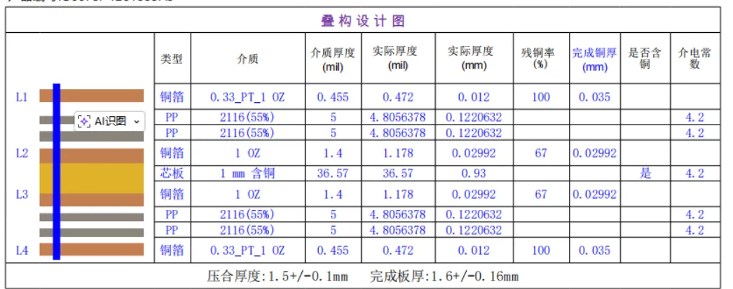
The inner layer names in the provided files did not clearly indicate the stacking sequence. Additionally, the fabrication notes specified 2.0mm board thickness, while the customer's stackup drawing showed 2.2mm. We noticed this discrepancy immediately after loading the files.
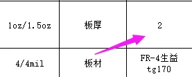
Figure 1: the fabrication notes specified 2.0mm board thickness
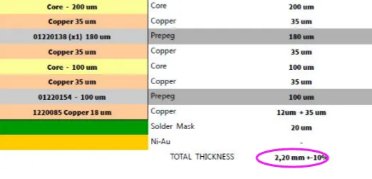
Figure 2: customer's stackup drawing showed 2.2mm
Our engineer asked for confirmation on the exact layer order and whether to follow the 2.2mm stackup. According to IPC-2221 guidelines for multilayer construction, correct layer sequencing is essential for maintaining registration and impedance consistency. If ignored, incorrect stacking could lead to severe registration errors, delamination, or complete signal integrity failure.
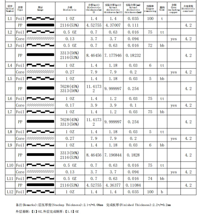
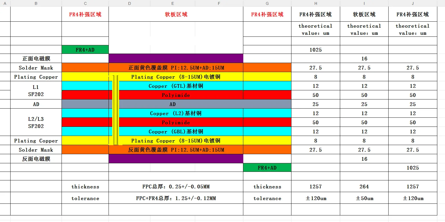
Figure 3: suggested PCB stackup
Proceeding without clarification risked producing boards with wrong dielectric thicknesses, resulting in impedance deviation far beyond acceptable limits and potential scrap of the entire lot. The customer confirmed the stackup sequence and 2.2mm thickness.
Missing Impedance Reference Data
Although impedance control was listed in the requirements, we could not find detailed reference traces, target values, or layer-specific information in the Gerber files or documentation. This is a common but critical gap in high-layer-count designs.
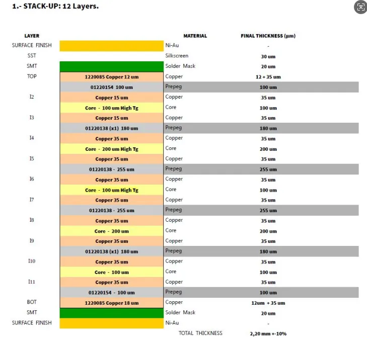
Figure 4: impedance reference data was not found
Without this data, accurate modeling becomes difficult. We had to flag this for confirmation because mismatched impedance control can cause signal reflections and timing issues in high-speed applications. If production had continued blindly, the final boards might have failed electrical testing, leading to costly rework or respins.
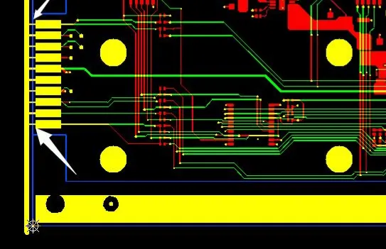
Edge Copper Clearance and Routing Exposure Risk
Several copper features were positioned too close to the board edge. During mechanical routing, this would likely result in exposed copper. We noticed this during the panelization and outline review and immediately raised an EQ asking for confirmation on how to handle these areas.
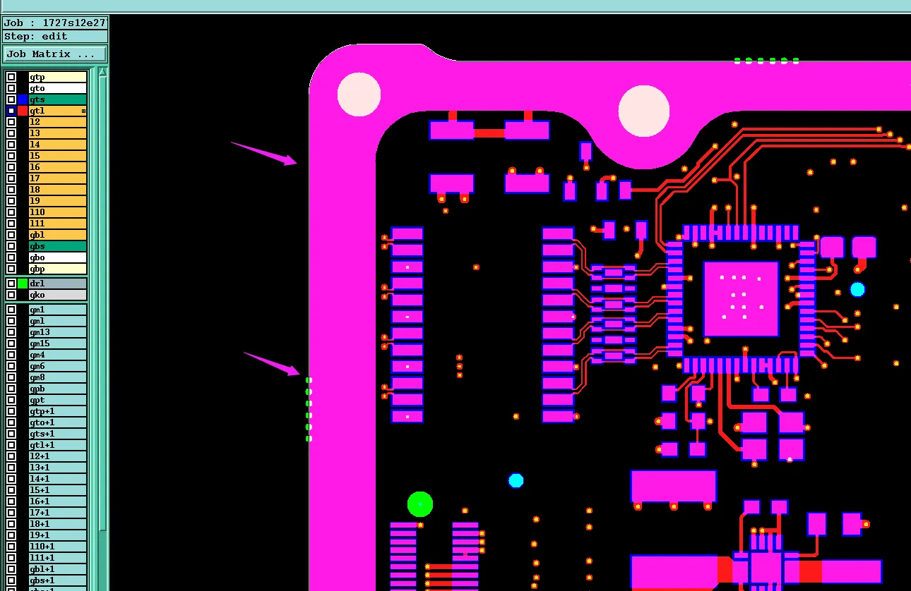
Figure 5: several copper features were positioned too close to the board edge
Based on IPC-A-600 acceptability criteria, exposed copper on edges significantly increases oxidation risk and can cause short circuits during assembly or field use. If not addressed, the boards could suffer from cosmetic defects, poor solderability at the edge, or even electrical shorts after depanelization.
Asymmetric Annular Rings and Outer Layer Copper Adjustment
We identified pads where one side had a proper annular ring while the opposite side had a pad size equal to the hole (no ring). Due to the 1.5oz outer copper weight and tight 4mil line/space, our negative film process required enlarging the annular ring on the no-ring side to ensure reliable plating and etching.
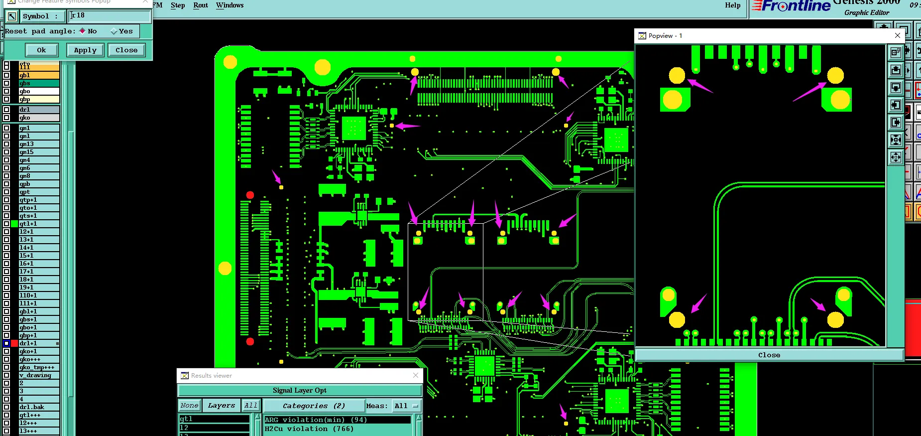
Figure 6: a pad size equal to the hole
Our CAM team confirmed this was consistent with previous production files. Without this adjustment, the risk of breakout, thin plating, or copper peeling would be very high, especially with 1.5oz copper. The customer approved the modification after reviewing our explanation.
Solder Mask Bridge and Drill-to-Line Clearance
Some pad-to-pad spacings were too tight for a reliable solder mask bridge, and several drill holes were too close to traces. We asked whether no-bridge conditions were acceptable and if traces could be adjusted for safe clearance.
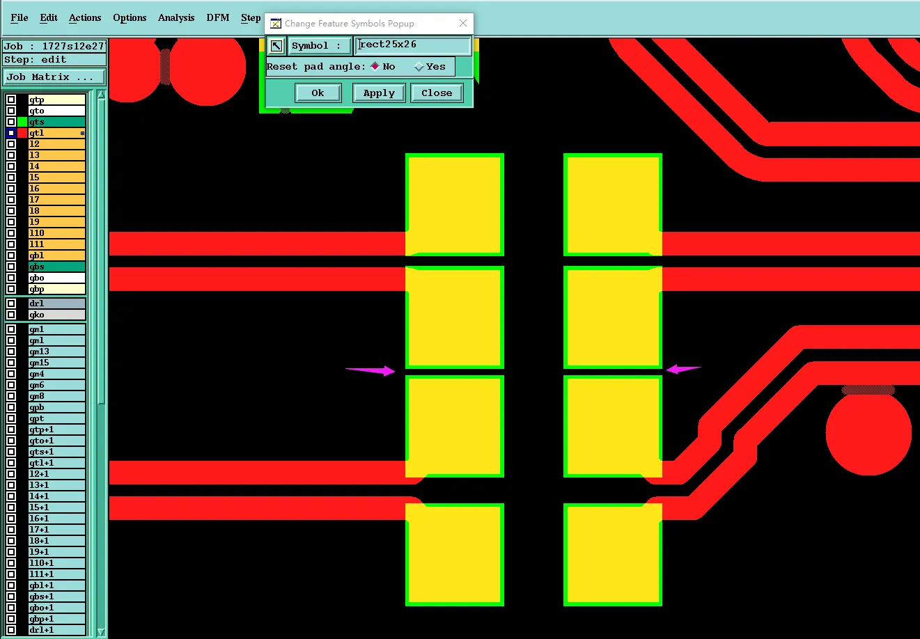
Figure 7: pad-to-pad spacings were too tight for a reliable solder mask bridge
These are common manufacturability limits. Ignoring them could result in solder mask voids, solder bridging during assembly, or drill breakout damaging adjacent copper.
Manufacturing Risks and DFM Insights
This case underscores how stackup documentation, edge clearances, and copper weight considerations frequently trigger EQs in 12-layer boards. Designers often overlook the real impact of 1.5oz outer copper on annular ring requirements and negative process limitations. Tight edge copper is another recurring issue that can cause exposed copper after routing.
If left unresolved, these problems commonly lead to registration failure, impedance deviation, edge shorts, reduced yield, and assembly defects. In similar past jobs, unconfirmed annular ring adjustments resulted in plating voids and significant scrap rates.
How the Engineering Team Resolved the Issues
Our team provided marked-up images for each issue and requested specific confirmations. For the stackup and thickness, we aligned production data exactly to the customer's provided drawing after approval. Edge copper areas were reviewed case-by-case, with adjustments made where necessary to prevent exposure.
We noticed the asymmetric pads would be problematic with 1.5oz copper, so our engineer recommended and received approval to enlarge rings on the no-ring side. All panel updates and file confirmations were processed after customer feedback. This structured clarification process minimized risk and avoided multiple revision cycles.
Final Manufacturing Outcome
All engineering questions were satisfactorily answered by the customer. Production files were updated with confirmed stackup order, 2.2mm thickness, approved annular ring modifications, and edge clearance handling. The order was approved for production with optimized DFM adjustments.
Key Takeaways for PCB Designers
- Always provide a clear layer stacking sequence diagram when inner layer names are not self-explanatory.
- Include detailed impedance reference traces, target values, and tolerance requirements directly in fabrication documentation.
- Maintain sufficient copper-to-edge clearance (typically >0.3mm) to prevent exposure after routing or scoring.
- Design symmetric annular rings, especially on thicker outer copper layers, to support reliable negative imaging processes.
- Verify minimum solder mask bridge capability against your chosen fabricator's rules before finalizing tight BGA or fine-pitch layouts.
- Account for actual manufacturable board thickness early, as it may differ from nominal values based on material and layer count.
- Provide complete, consistent stackup files and clearly state whether modifications are allowed.
FAQ
Q1: Why is layer stacking sequence clarification important in multilayer PCBs?
A1: Incorrect layer order can cause registration misalignment, impedance errors, and delamination. Proper sequencing ensures reliable drilling, plating, and electrical performance across all layers.
Q2: What happens if copper features are too close to the board edge?
A2: Mechanical routing may expose copper, leading to oxidation, shorts, or cosmetic rejection. Confirming clearances prevents edge defects that could cause field failures.
Q3: Why do factories sometimes enlarge annular rings on one side?
A3: With thicker outer copper (e.g. 1.5oz) and tight tolerances, negative process requirements may necessitate ring enlargement to ensure adequate plating and etching reliability.
Q4: Can board thickness differ from the specified value?
A4: Yes, when the provided stackup drawing shows a different value. Following the detailed stackup usually takes priority to maintain impedance and structural integrity.
Q5: What is the risk of missing impedance details in fabrication files?
A5: Without reference traces and targets, the factory cannot reliably model or verify impedance, potentially resulting in boards that fail high-speed performance requirements.