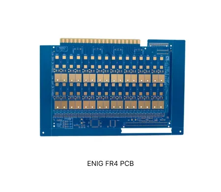
ENIG FR4 PCB Production Record #FR4-20260117-008
| Parameter | Value | Parameter | Value |
|---|---|---|---|
| PCB Type | FR4 PCB | Quantity | 5 pcs |
| Layers | 12 Layers | Board Type | Panel PCB |
| Dimensions | 82.01 x 100 mm | Copper Weight | 1.5oz |
| Thickness | 2 mm | Min Track / Spacing | 4/4mil |
| Surface Finish | ENIG (Immersion Gold) | Min Hole Size | 0.1mm |
| Solder Mask | Green | Silkscreen | White |
| Stack-up | Custom | Impedance Control | Yes |
This 12-layer FR-4 board (82.01 × 100 mm, 2.2 mm finished thickness, TG170 S1000-2M material) was built as a single-unit panel for a quantity of 5 pieces. Outer copper was 1 oz on one side and 1.5 oz on the other, with 4 mil minimum line/space, 0.1 mm minimum hole size, and full 100% flying probe testing. The order required impedance control, ENIG surface finish, green solder mask, white legend, and routed outline with 4 mm process edges on all sides. No resin plugging or gold fingers were specified.
DFM review identified several critical clarifications. Inner layer naming did not clearly indicate stackup sequence, requiring customer confirmation for correct lamination order. Edge copper features were positioned too close to the board outline, risking copper exposure during routing. Pad geometry showed annular ring asymmetry, with one side lacking sufficient ring; due to the 1.5 oz outer copper and tight geometries, we enlarged the ring on the equal-pad side to support reliable negative imaging. We also addressed tight drill-to-line clearances by trace adjustment and confirmed stackup thickness at 2.2 mm per the press sheet. These points, along with solder bridge acceptance on tight pads and impedance documentation gaps, were resolved through direct file updates and panel revisions. stackup clarification and annular ring asymmetry followed our standard engineering controls for high-layer count boards.
All engineering questions received customer confirmation before production release. The order completed within the 15-day delivery window using mechanical forming. Final electrical testing and quality documentation verified compliance with the adjusted parameters and controlled processes.
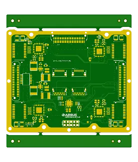
FR4 material with ENIG finish provides balanced electrical performance, shelf life, and assembly compatibility for industrial and high-reliability electronics.
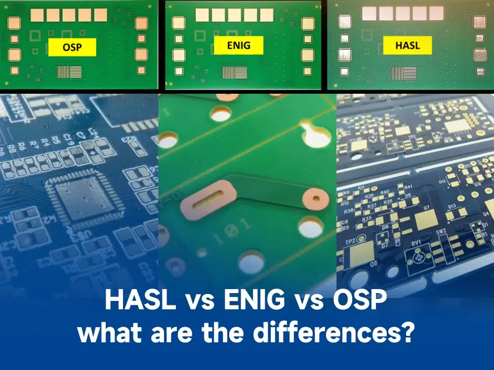
Explore common engineering queries in ENIG, HASL, and OSP FR4 PCBs. Learn real DFM challenges, surface finish compatibility issues, and practical solutions to reduce manufacturing risks and improve yield.
| Order ID | PCB Type | Layers | Dimensions | Solder Mask | Surface Finish | Quantity | Action |
|---|---|---|---|---|---|---|---|
| FR4-20260630-014 | FR4 PCB | 2 | 126 x 145 | Green | ENIG (Immersion Gold) | 10 | View detail |
| FR4-20260529-059 | FR4 PCB | 2 | 147.3 x 53.8 | Green | ENIG (Immersion Gold) | 5 | View detail |
| FR4-20260520-046 | FR4 PCB | 2 | 94.21 x 275 | Green | ENIG (Immersion Gold) | 75 | View detail |


