










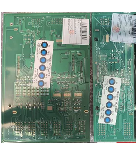
PCB Specifications
| Parameter | Value | Parameter | Value |
|---|---|---|---|
| PCB Type | FR4 PCB | Quantity | 75 pcs |
| Layers | 2 Layers | Board Type | Panel PCB |
| Dimensions | 94.21 x 275 mm | Copper Weight | 1oz |
| Thickness | 2.4 mm | Min Track / Spacing | 6/6mil↑ |
| Surface Finish | ENIG (Immersion Gold) | Min Hole Size | 0.3mm↑ |
| Solder Mask | Green | Silkscreen | White |
| Stack-up | Custom | Impedance Control | No |
Manufacturing Timeline
Logistics Information
Key Manufacturing Processes
Manufacturing Summary
For this order we manufactured 75 units of 2-layer FR4 panel PCBs using a custom stackup, 1 oz copper, and 2.4 mm overall thickness. The elongated 94.21 × 275 mm format required precise material preparation and lamination control to maintain flatness and dimensional accuracy across the panels. With standard 6/6 mil trace spacing and 0.3 mm minimum holes, circuit imaging and etching followed conventional parameters, delivering clean geometries without requiring advanced geometry techniques.
Green soldermask and white silkscreen were applied prior to electroless nickel and immersion gold deposition, producing a uniform ENIG surface finish that supports reliable soldering and corrosion resistance. Electrical testing verified continuity and isolation on every panel. Completed in 4.6 days from engineering review through final inspection, the run demonstrated steady process control for these thicker, extended panel boards.
This order also received positive feedback from the customer regarding the consistent quality and reliable delivery. View the full customer review→
Explore More PCB Manufacturing Resources
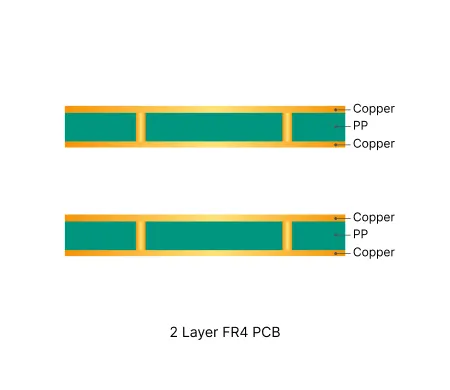
2 Layer FR4 PCB Manufacturing Insights
2 layer FR4 PCBs deliver cost-effective solutions for most electronic designs. Their simple structure enables consistent quality and efficient production cycles.
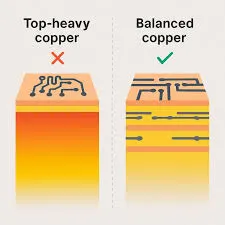
Why 1 Layer and 2 Layer FR4 PCB Trigger Frequent Engineering Queries in Production
Real Engineering Queries (EQ) and DFM issues for 2 Layer FR4 PCB (double-sided boards) from actual production reviews. Learn how to avoid common problems with via treatment, silkscreen on pads, solder mask openings, hole attributes, board edge clearance, and other frequent design pitfalls.
Real Production Records
| Order ID | PCB Type | Layers | Dimensions | Solder Mask | Surface Finish | Quantity | Action |
|---|---|---|---|---|---|---|---|
| FR4-20260910-004 | FR4 PCB | 2 | 69.92 x 69.91 | White | HASL Lead Free | 5 | View detail |
| FR4-20260907-001 | FR4 PCB | 2 | 90 x 40 | Green | HASL Lead Free | 30 | View detail |
| FR4-20260905-007 | FR4 PCB | 2 | 42.8 x 38.8 | Green | HASL Lead Free | 5 | View detail |


