 00:42
00:42
PCB Trace Spacing
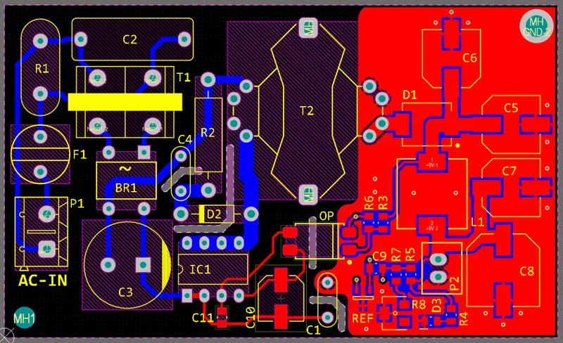
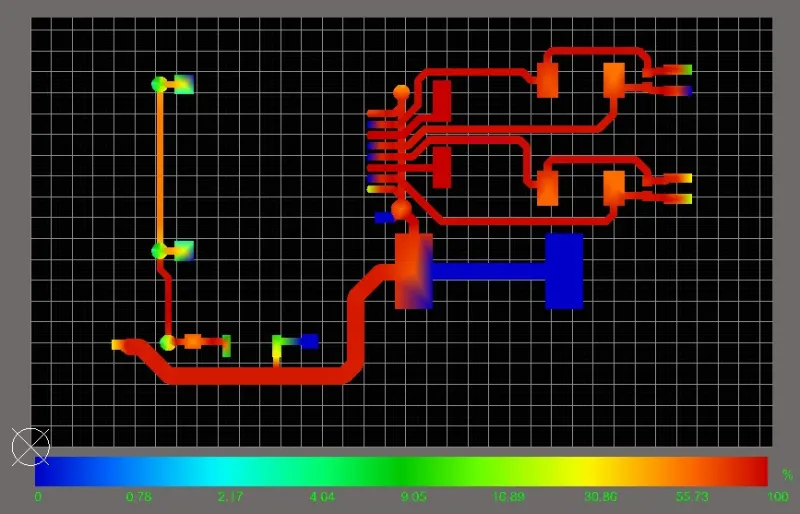
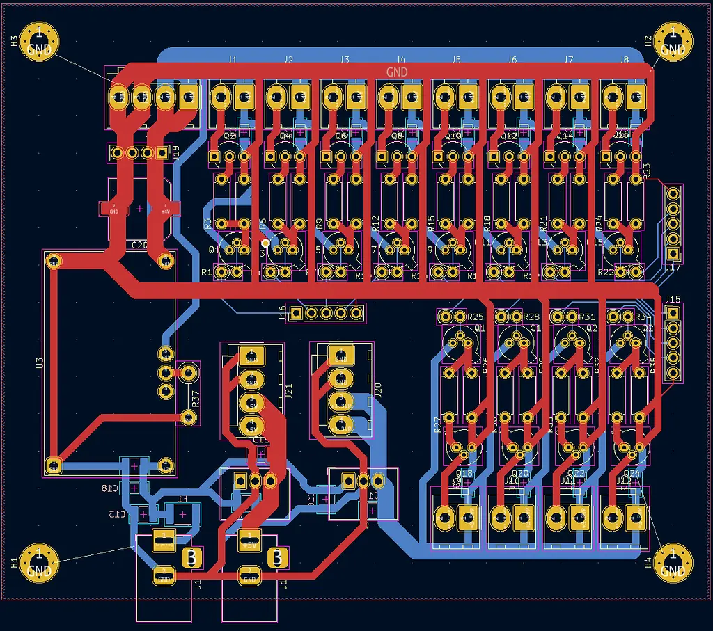
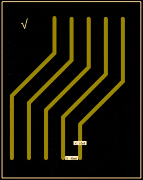
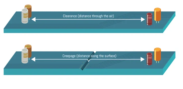
PCB trace spacing is a critical aspect of printed circuit board design that ensures electrical reliability, safety, and performance. This tag encompasses a range of topics related to the minimum distances required between conductive traces, pads, and other components on a PCB. Proper spacing prevents issues such as electrical arcing, signal interference, and short circuits, which can lead to system failures or safety hazards. For engineers and designers searching for PCB trace spacing guidelines, this collection of articles provides essential knowledge on standards like IPC-2221, which outline clearance and creepage distances based on voltage levels, environmental conditions, and board materials. Understanding PCB trace spacing starts with recognizing its role in high-voltage applications, where wider gaps are necessary to avoid dielectric breakdown, versus low-voltage digital circuits that prioritize dense layouts for miniaturization. Practical applications include calculating spacing for power electronics, RF designs, and multilayer boards, where factors like humidity, altitude, and pollution degrees influence the requirements. Best practices involve using design software tools to simulate and verify spacing rules, incorporating safety margins to account for manufacturing tolerances, and adhering to regulatory compliances such as UL or IEC standards to ensure product certification. For those tackling specific challenges, such as optimizing trace spacing in compact IoT devices or high-speed PCBs, the articles under this tag offer actionable insights. They discuss common pitfalls, like underestimating thermal expansion effects or ignoring via-to-trace clearances, and provide step-by-step methods for implementation. Readers can find detailed explanations of formulas for minimum spacing, real-world case studies, and tips for prototyping to validate designs. By exploring these resources, designers gain the tools to create robust PCBs that meet performance goals while minimizing risks.
Video Guide
-
00:42
Technical Articles
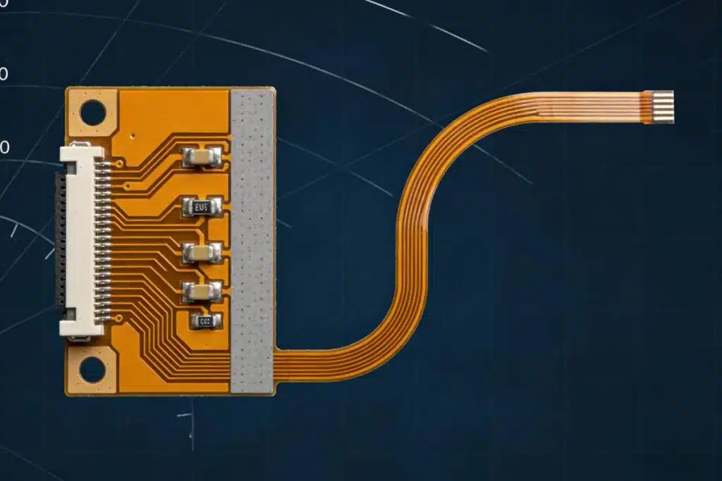
How Much Clearance Between FPC Trace and Board Edge Is Safe?
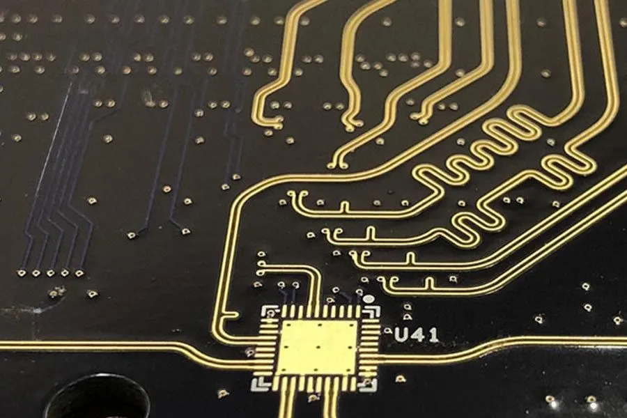
What are PCB Traces?
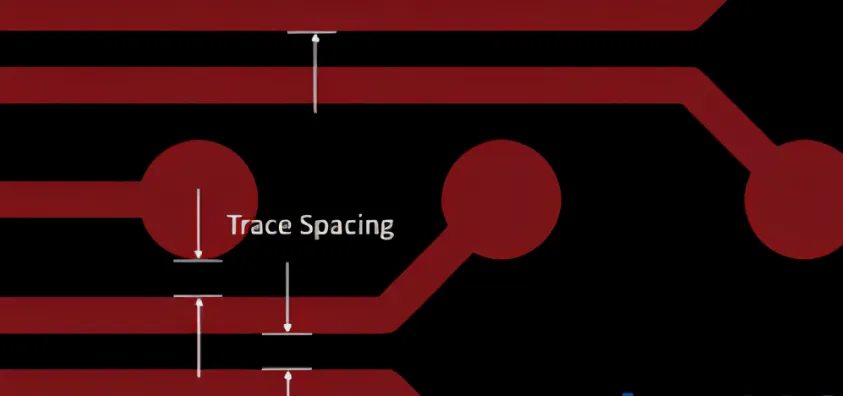
The Ultimate Guide to Minimum Trace Spacing: Ensuring Signal Integrity and Preventing PCB Failures
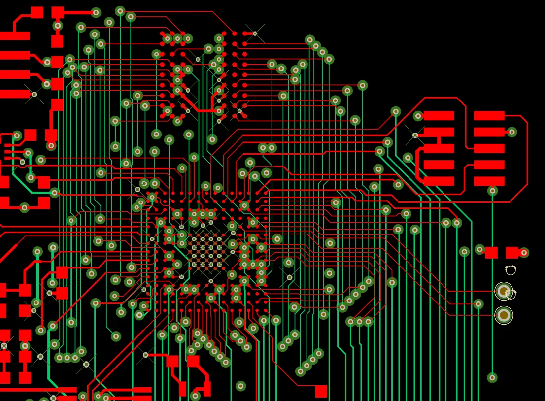
Signal Integrity and Minimum Trace Spacing: Optimizing PCB Layout for High Speed Designs
High Voltage PCB Design: Mastering Minimum Trace Spacing for Safety and Performance
Optimize Your CEM 1 PCB Design: Mastering Trace Width and Spacing
Spacing Secrets: Mastering Trace Width for High Voltage PCBs
How to Calculate Optimal Trace Spacing in PCB Design
Optimizing PCB Trace Clearance: A Guide to Reliable Circuit Board Design
The Art of PCB Trace Routing: Techniques for Reducing Crosstalk and Noise
Get in Touch
Send Message
- Products & Service
- Company
- About AIVON
- Contact
- News
- Blog
- Certification
-


- Payment
-


2026 AIVON.COM All Rights Reserved